


Project Log
I will be creating the production PC Board for Steve's thread:
https://www.electronicspoint.com/th...chematic-yet-another-work-in-progress.256843/
I thought while I was at it, why not do a DIY one as well?
So here goes.
I will use ExpressPCB's free software to design the PC board. This is proprietary software from a PCB manufacturer that I have used. The software is beautifully simple and easy to use, so it is great for a hobbyist.
I will be using a laser printer to print out the copper pattern, then using an iron to transfer the pattern to a copper clad board.
I will then etch the board using Ferric Chloride. Next I remove the resist with nail polish remover, drill the holes with a Dremel tool in a drill press jig, and finally assemble the board.
I will post an additional message for each step in the process.
Bob
Step 1. Enter the schematic.
Although you could lay out the PC board without entering the schematic, it is much simpler if you do. The software will know where all the connections need to be and check them for you.
For this project I am using the free software from ExpressPCB, which you can get here: ExpressPCB CAD software
Then enter the schematic. The user interface is quite natural, I find. It has a lot of built-in parts and packages defined and it is very easy to create your own custom components. Here is the schematic as entered to ExpressPCB.
Note that I have made a couple of changes from Steve's schematic. I am going to put 2 little 20ma LEDs on the board, so the series resistor for them has been increased to 220R. Also, I have added a connector for power. You normally would not need to show this on the schematic, but when putting it on a PC board, you must have everything you are going to put on the board.
Also, I have changed the MOSFET to a VN3205 which is a TO92 1A mosfet with 0.3R on resistance that I happen to have in my parts box.

Step 2. Lay out the PC board.
I will not go into detail here because it is a long and laborious process. For my DIY board, I am sticking to 1 sided, which makes layout a lot more difficult. By persisting and moving parts around a lot, I was able to make all the connections with a one-sided board with no jumpers.
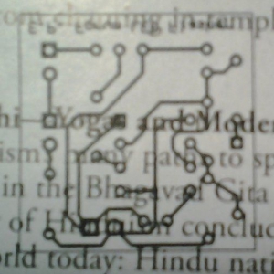
Here is the final layout. This may look huge to you, but it is a one inch square! The green is the bottom copper layer. The yellow is the silk-screen layer, which just labels all of the parts on the top of the board. I used 15 mil (thousandth of an inch) traces and kept the spacing at that at least. For my DIY process, I can go a little smaller than this, but not much. In a production board these traces would be considered huge.
When you layout the PCB layout, you give the software the schematic. You then add parts to the board, and they are linked to the schematic by having the same name. I.e. R1 on the schematic must be labelled as R1 on the board. Once you have placed the parts on the board, you can select the "highlight connections" tool, and when you click on any solder pad it will highlight all the other pads that are connected to it. You then draw the wires between them. Finally, you check to make sure all pads are connected as they should be, by clicking on each pad and following your traces to make sure all the right pads and none of the wrong pads are connected.

Step 3. Transferring the layout to a copper clad board.
Use the PC layout software to print just the bottom copper layer on a laser printer. Note that it must be a laser printer, an ink-jet will not work. Why? Because the laser printer melts plastic onto the page to print. You will then transfer this plastic to your copper clad board, by using a clothes iron. The plastic will prevent copper from being etched away and leave copper in the pattern you have designed.
I have tried every kind of paper for this transfer. Plain paper, high gloss laser printer paper, very expensive blue plastic image transfer sheets, and flimsy cheap semi-glossy paper from catalogs.
Which works the best? You got it, the flimsy junk mail! Why? Not sure, but I think it has just enough gloss to keep the toner from soaking into the paper and is flimsily enough to fall apart and leave the toner behing when you soak it.
So here is the process:
1. Print the copper onto junk mail catalog paper. It doesn't matter that there is print or pictures on the paper. The ink will not transfer, only the laser toner.
2. Polish the portion of the copper clad board with a Scotch-Brite pad (nylon dish scrubbing pad).
3. Cut the paper in the shape of the board, leaving extra on one side. Tape that extra portion to the copper-clad board, image side down. Do not tape over the image or you will melt the tape with the iron.
4. Set an iron near the high end of temperature, but not quite. You will have to experiment. Place the board with image on a piece of plywood. Run the iron over it for several minutes putting a bit of pressure and making sure you hit all areas. This is difficult to get right, but experiment with the temp, time and pressure until you get good results.
5. Under running warm water, gently rub the paper until it come off. Hopefully, it leaves a perfect image of your board layout.
6. Inspect the image to make sure there are not missing parts, and no traces have flowed together, which happens if you get it too hot. If it is not good, remove the image with the Scotch-Brite and go back to step 1.
7. I use a band saw to cut the board to the final shape, and then file the edges smooth.


Step 4. Etching.
This is as simple as it gets. I use PCB etchant (ferric chloride) that I bought at Radio Shack. I do the etching in a Zip-lock plastic food storage container. I can use the etchant over and over again for the small boards I make, and I just keep in covered in the Zip-lock.
I use a pair of wood sticks with a little notch and a rubber band to hold the board, then I just swish it around in the etchant for 15 minutes or so until all the excess copper is gone. I then wash it, and remove the toner using nail polish remover. Again, inspect the board to make sure all the traces are there and and there are no bridges. (I fix minor breaks with a bit a wire soldered across them if I can. In this case, there were none, it came out perfect.)


Step 5. Drill.
I use a Dremel tool in a Dremel drill press jig. I use double sided tape to tape the board to a piece of plywood so it has backing for the drilling and is easier to manipulate. I use magnifier on a headband so that I can hit the holes accurately.
In this case, I should have made the pads a little large. If drilled out part of the pad on a few of the hole. But each hole ended up with enough copper around it to successfully solder, so no harm.
After drilling, I print and transfer the silk screen layer to the top of the board. This shows me where all the parts go. The tricky thing about this, though, is you have to mirror the image before printing it. The bottom copper layer was already mirrored because it is on the back of the board, and the print is from the front. I clipped the image from the PCB layout program and then mirrored it with a photo editing program. I smudged this a little when ironed it on, but it is still usable so I left it.

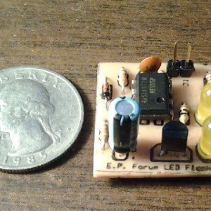
Step 6. Populate and solder.
Here is the final result:


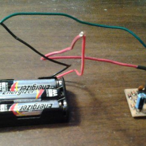
Step 7. Connect power.
Holy Cow! It is flashing at a rate of about once per second, as designed!

https://www.electronicspoint.com/th...chematic-yet-another-work-in-progress.256843/
I thought while I was at it, why not do a DIY one as well?
So here goes.
I will use ExpressPCB's free software to design the PC board. This is proprietary software from a PCB manufacturer that I have used. The software is beautifully simple and easy to use, so it is great for a hobbyist.
I will be using a laser printer to print out the copper pattern, then using an iron to transfer the pattern to a copper clad board.
I will then etch the board using Ferric Chloride. Next I remove the resist with nail polish remover, drill the holes with a Dremel tool in a drill press jig, and finally assemble the board.
I will post an additional message for each step in the process.
Bob
Step 1. Enter the schematic.
Although you could lay out the PC board without entering the schematic, it is much simpler if you do. The software will know where all the connections need to be and check them for you.
For this project I am using the free software from ExpressPCB, which you can get here: ExpressPCB CAD software
Then enter the schematic. The user interface is quite natural, I find. It has a lot of built-in parts and packages defined and it is very easy to create your own custom components. Here is the schematic as entered to ExpressPCB.
Note that I have made a couple of changes from Steve's schematic. I am going to put 2 little 20ma LEDs on the board, so the series resistor for them has been increased to 220R. Also, I have added a connector for power. You normally would not need to show this on the schematic, but when putting it on a PC board, you must have everything you are going to put on the board.
Also, I have changed the MOSFET to a VN3205 which is a TO92 1A mosfet with 0.3R on resistance that I happen to have in my parts box.
Step 2. Lay out the PC board.
I will not go into detail here because it is a long and laborious process. For my DIY board, I am sticking to 1 sided, which makes layout a lot more difficult. By persisting and moving parts around a lot, I was able to make all the connections with a one-sided board with no jumpers.
Here is the final layout. This may look huge to you, but it is a one inch square! The green is the bottom copper layer. The yellow is the silk-screen layer, which just labels all of the parts on the top of the board. I used 15 mil (thousandth of an inch) traces and kept the spacing at that at least. For my DIY process, I can go a little smaller than this, but not much. In a production board these traces would be considered huge.
When you layout the PCB layout, you give the software the schematic. You then add parts to the board, and they are linked to the schematic by having the same name. I.e. R1 on the schematic must be labelled as R1 on the board. Once you have placed the parts on the board, you can select the "highlight connections" tool, and when you click on any solder pad it will highlight all the other pads that are connected to it. You then draw the wires between them. Finally, you check to make sure all pads are connected as they should be, by clicking on each pad and following your traces to make sure all the right pads and none of the wrong pads are connected.
Step 3. Transferring the layout to a copper clad board.
Use the PC layout software to print just the bottom copper layer on a laser printer. Note that it must be a laser printer, an ink-jet will not work. Why? Because the laser printer melts plastic onto the page to print. You will then transfer this plastic to your copper clad board, by using a clothes iron. The plastic will prevent copper from being etched away and leave copper in the pattern you have designed.
I have tried every kind of paper for this transfer. Plain paper, high gloss laser printer paper, very expensive blue plastic image transfer sheets, and flimsy cheap semi-glossy paper from catalogs.
Which works the best? You got it, the flimsy junk mail! Why? Not sure, but I think it has just enough gloss to keep the toner from soaking into the paper and is flimsily enough to fall apart and leave the toner behing when you soak it.
So here is the process:
1. Print the copper onto junk mail catalog paper. It doesn't matter that there is print or pictures on the paper. The ink will not transfer, only the laser toner.
2. Polish the portion of the copper clad board with a Scotch-Brite pad (nylon dish scrubbing pad).
3. Cut the paper in the shape of the board, leaving extra on one side. Tape that extra portion to the copper-clad board, image side down. Do not tape over the image or you will melt the tape with the iron.
4. Set an iron near the high end of temperature, but not quite. You will have to experiment. Place the board with image on a piece of plywood. Run the iron over it for several minutes putting a bit of pressure and making sure you hit all areas. This is difficult to get right, but experiment with the temp, time and pressure until you get good results.
5. Under running warm water, gently rub the paper until it come off. Hopefully, it leaves a perfect image of your board layout.
6. Inspect the image to make sure there are not missing parts, and no traces have flowed together, which happens if you get it too hot. If it is not good, remove the image with the Scotch-Brite and go back to step 1.
7. I use a band saw to cut the board to the final shape, and then file the edges smooth.
Step 4. Etching.
This is as simple as it gets. I use PCB etchant (ferric chloride) that I bought at Radio Shack. I do the etching in a Zip-lock plastic food storage container. I can use the etchant over and over again for the small boards I make, and I just keep in covered in the Zip-lock.
I use a pair of wood sticks with a little notch and a rubber band to hold the board, then I just swish it around in the etchant for 15 minutes or so until all the excess copper is gone. I then wash it, and remove the toner using nail polish remover. Again, inspect the board to make sure all the traces are there and and there are no bridges. (I fix minor breaks with a bit a wire soldered across them if I can. In this case, there were none, it came out perfect.)
Step 5. Drill.
I use a Dremel tool in a Dremel drill press jig. I use double sided tape to tape the board to a piece of plywood so it has backing for the drilling and is easier to manipulate. I use magnifier on a headband so that I can hit the holes accurately.
In this case, I should have made the pads a little large. If drilled out part of the pad on a few of the hole. But each hole ended up with enough copper around it to successfully solder, so no harm.
After drilling, I print and transfer the silk screen layer to the top of the board. This shows me where all the parts go. The tricky thing about this, though, is you have to mirror the image before printing it. The bottom copper layer was already mirrored because it is on the back of the board, and the print is from the front. I clipped the image from the PCB layout program and then mirrored it with a photo editing program. I smudged this a little when ironed it on, but it is still usable so I left it.
Step 6. Populate and solder.
Here is the final result:
Step 7. Connect power.
Holy Cow! It is flashing at a rate of about once per second, as designed!