Maker Pro
Maker Pro

Creating logic AND gate with 2N222 Transistor

SmapaPurf

Jul 19, 2016
1
Joined
Jul 19, 2016
Messages
1
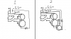
i have been trying to build a simple AND gate with 2N222 transistor but when i assemble the parts like so (Schematic 1) when the second transistor in the series is activated but not the first the small current flowing through lights the LED dimly,this bothered be so i made a second design hoping to fix this but made the issue worse(Schematic 2) as now the small current from base to emitter activate next transistor controlling the LED.How can i make the LED not be dimly lit via the base-emitter flow?
 

Attachments

  • schem AND.png
    schem AND.png
    38.2 KB · Views: 257

BobK

Jan 5, 2010
7,682
Joined
Jan 5, 2010
Messages
7,682
Move the LED to between the top collector and the positive supply.

Bob
 

Sunnysky

Jul 15, 2016
541
Joined
Jul 15, 2016
Messages
541
in the 1st circuit, a Large 100k~1MΩ resistor from base to ground (V-), shunts stray e-field leakage and allows it turn off LED.

Otherwise , waving hand near circuit makes it brighter when both sw. off.
Put on both bases to V- for best results.
 

BobK

Jan 5, 2010
7,682
Joined
Jan 5, 2010
Messages
7,682
Sunny.

His problem is that when the second input is activated, the LED sees the base-emitter current through the second transistor. Moving the LED to the collector as I suggested would solve this problem.

Not that a pulldown is not a good idea as well.

Bob
 

AnalogKid

Jun 10, 2015
2,893
Joined
Jun 10, 2015
Messages
2,893
1. Separate 4.7K series resistors to each base.
2. Large resistor (100K to 470K) from each base to GND.

ak
 

Sunnysky

Jul 15, 2016
541
Joined
Jul 15, 2016
Messages
541
You are quite correct Bob . This also lowers the input voltage threshold from 2.7, which is ~Vbat/2 to 0.7V approx. and works.

Smurph->
Logic designs for TTL have been around for eons but the standards for input voltage threshold have never changed for TTL. I suggest you follow Bob's mod and you may* add Vbe equal or larger value resistors to gnd to shunt stray noise.

Google images will show many ways to make TTL AND and NAND gate schematics.
±

tickytackytechnical question

For the expert interview question, or who wants to be a millionare final question, what is the value you expect for input threshold of all TTL (at room temp) between 0 and 1 ?. the exact voltage... not the recommended range for 0&1 but the one and only answer (0.1V tolerance acceptable on your answer)... drum roll please....

74xx, 74Sxx, 74LSxx, 74Lxx families of TTL and also some CMOS adopted this as well but not CD4000 or 74HCxx...
 
Last edited:

BobK

Jan 5, 2010
7,682
Joined
Jan 5, 2010
Messages
7,682
Not cheating. From memory 0.8 and 2.5?

Bob
 

Sunnysky

Jul 15, 2016
541
Joined
Jul 15, 2016
Messages
541
nope. It is a single value , like a comparator with its refernce voltage.
What is that TTL threshold?

Hint if you measure the floating input, it happens to be a logic 1 if you see the output, but floating input is very close to the input threshold, which is the answer I expect.

next contestant, or I'll make an exception with 3 guesses if justified.. ALL TTL families work this way, inspite of various implementations.

Hint 2 you wont find it in the table of values in the datasheet.
This is a question based ln experience and ability to read schematics.

For bonus points, the reason why TTL thresholds are defined as 0.8 & 2.0 for 0&1 respectively in "two or three words"
 
Last edited:

BobK

Jan 5, 2010
7,682
Joined
Jan 5, 2010
Messages
7,682
Okay, I read you question too quickly. I was giving the acceptable low (< 0.8) and high (>2.5) levels, and I got that wrong, the high is 2.0.

I have never heard of a threshold voltage, I have always thought anything between 0.8 and 2.0 gave undefined results.

Bob
 

Sunnysky

Jul 15, 2016
541
Joined
Jul 15, 2016
Messages
541
if you can read schematics on " google images" for ttl, you will know.
This is why I included this question in all my interviews for design engineers.
 

AnalogKid

Jun 10, 2015
2,893
Joined
Jun 10, 2015
Messages
2,893
From memory, 1.8 V. This is the terminal voltage of a floating TTL input pin.

ak
 

Sunnysky

Jul 15, 2016
541
Joined
Jul 15, 2016
Messages
541
Nobody got close to the correct answer.

The floating input voltage threshold for TTL in every generation is two base-emitter diode drops or 0.65x2 =1.3V. The voltage needed to pull the floating input down to cause an output transition is about 0.1~0.2V.

so 1.2 ±0.1

The same "rated " thresholds have existed in all TTL families of 0.8 and 2.0 are rated for equal noise immunity , which for voltage would average to 1.4V, but because the input load current is asymmetrical, the threshold 1 is higher to demand equal "noise power" margin from equal immunity.
 

(*steve*)

¡sǝpodᴉʇuɐ ǝɥʇ ɹɐǝɥd
Moderator
Jan 21, 2010
25,510
Joined
Jan 21, 2010
Messages
25,510
At 1.3V +/- 0.1V do you get?

The specified output voltage levels?

The specified propagation delays?

Operation over the specified range of power supply voltages and ambient temperatures?
 

Sunnysky

Jul 15, 2016
541
Joined
Jul 15, 2016
Messages
541
At 1.3V +/- 0.1V do you get?

The specified output voltage levels?

The specified propagation delays?

Operation over the specified range of power supply voltages and ambient temperatures?

not relevant.. also Vout is not affected due to saturation and gain.

This question shows you thoroughly understand EMC and can read schematics for transistor ccts and estimate voltages, tests your experience on floating inputs, and shows you understand about noise immunity what it means, for this so called grey zone between 0.8 & 2V

When observing valid input levels vs output at speed, you can see the input transition current occurs at this threshold and understand what stray current is needed too overcome signal from noise on input atthis threshold and decide when you need Schmitt inputs or not.

It also shows if you gave designed a series mode Xtal or LC TTL oscillator.

So it is a simple test of advanced experience.

In the end, all logic gates are analog devicesm when it comes to bias and noise immunity, etc.

Each TTL family has different speed and power attributes but all the same Vin threshold and thus same "valid" levels of 0.8 &2.0 for normal immunity, which assumes a. ertain level ov crosstalk and signal. noise on cables.
 
Top