Barathbushan,thank you four your explaination.
I have a few questions for you:
First I agree with your explaination why are used cmos transmission gates in this circuit.
I need to prove why this circuit can't work with overlapping clocks.
You said that with overlapping clocks in this circuit only nmos transistors are conducting and that is the reason why this circuit can't work as dynamic shift register?
I don't understand that because that's not prove.
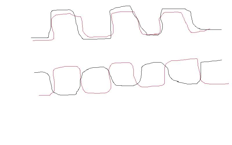
At the output of the second inverter when I simulated this circuit I get smaller voltage
then Vdd(Vdd=5v).I get 2.5V,and there is I have problem when I used overlapping clocks.
I don't know why is this happening.
Looking at the first inverter input, the inverter’s input will be whatever is at ''Vin'' when
Phi = 1. However, when Phi1 = 0, there is no logic level since the CMOS switch will be off. In a real transistor there will be parasitic capacitance that maintains charge and keeps the logic level at what it was when the CMOS switch was on.


") I'll send you a private message with the details of where I think you were in error.
I'll send you a private message with the details of where I think you were in error.