Maker Pro
Maker Pro

postive edge triggered D flipflop

bhuvanesh

Aug 29, 2013
201
Joined
Aug 29, 2013
Messages
201
In the above circuit if clock(CLK 1) goes from 0 to 1 and input D =0 ,this makes Q=0.
It is stated that when the clock is at HIGH(1) any further change in input does not affect output,how it is so .Can you explain me please.Thank you in advance
 

Attachments

  • pe_d_flipflop.png
    pe_d_flipflop.png
    36.6 KB · Views: 6,661

Harald Kapp

Moderator
Moderator
Nov 17, 2011
13,722
Joined
Nov 17, 2011
Messages
13,722
Find out for yourself:
1) draw all states (logic levels) with Clock=0 and Data=0.
2) beginning with the states from 1, draw all logic levels for clock=1 (this is the transistion of the positive clock edge)
3) from the states you drew in 2, consider all states if data changes from 0 to 1. Look especially at the inputs and outputs of the two rightmost NAND gates

You will find that some states change, some not. Those that do not change make the flipflop work as required.
 

bhuvanesh

Aug 29, 2013
201
Joined
Aug 29, 2013
Messages
201
My doubt start at very beginning.I have added notation to the image and uploaded, see this image
Consider clk 1(transfered from 0 to 1) and input data =0
In the image what is the input value for A nand gate and C nand gate.For clearance i marked that line with red.how to predict that input values.Please explain me that part.Thank you
 

Attachments

  • anoted diagram.png
    anoted diagram.png
    38.6 KB · Views: 447

Harald Kapp

Moderator
Moderator
Nov 17, 2011
13,722
Joined
Nov 17, 2011
Messages
13,722
That's a good start, but go back one step where clock is still "0", What's the value on the red line in this case? Does it change, and if so, how, when clock goes from "0" to "1"?
 

bhuvanesh

Aug 29, 2013
201
Joined
Aug 29, 2013
Messages
201
i am not native english speak.Do you pointing that red line values depends on past history
 

Harald Kapp

Moderator
Moderator
Nov 17, 2011
13,722
Joined
Nov 17, 2011
Messages
13,722
Yes. That is the idea of a flipflop: remember the history, e.g. the value of DATA just before the rising edge of CLOCK.
 

bhuvanesh

Aug 29, 2013
201
Joined
Aug 29, 2013
Messages
201
ok ,in case you buy a new flip flop which has no past values then what do u do.Do u manually reset it and start form that or do something else
 

Harald Kapp

Moderator
Moderator
Nov 17, 2011
13,722
Joined
Nov 17, 2011
Messages
13,722
When you power up a flipflop (apply power supply), the initial state is undefined. It depends on tiny variations in the device's components. Some flipflops will almost always turn on with Q=1, others with Q=0, others again with sometimes Q=1, sometimes Q=0.

That is the reason why many flipflops have a reset input.

In bad cases the flipflop can even be unstable and take an arbitrary time to settle into a stable state. This is called metastability and can lead to very unexpected timing errors.

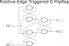
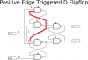
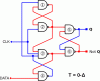
In your case, however, you should not consider metastability. You can analyze the circuit in terms of stable "0" and "1" states of the different gates. If you want to make sure you have understood the behavior correctly, analyze all 4 cases:
1) clock=0, previous state is Q=0, data=0, clock goes from 0->1
2) clock=1, previous state is Q=1, data=0, clock goes from 0->1
3) clock=0, previous state is Q=0, data=1, clock goes from 0->1
4) clock=1, previous state is Q=1, data=1, clock goes from 0->1
This is going to be some boring work but it will help you understand the operation of a flipflop.

Take some time and read this educational material on the operation of latches and flipflops, too.
 

Laplace

Apr 4, 2010
1,252
Joined
Apr 4, 2010
Messages
1,252
D-FF-EdgeTgr_anim.gif

When analyzing edge-triggered devices with memory it is more than just a static-logic problem. Internal propagation delays and race conditions may determine exactly how the device behaves. So I created this edge-triggered circuit in Libre Office Draw with the condition that all lines connected to a source node be grouped so that changing line color becomes much simpler. RED = Logic 1, BLUE = Logic 0. Then created views at sequential time deltas where Δ= propagation time through one gate. At time T=0 there is a positive clock edge; at time T=½ the clock signal returns to zero.

So just looking at the condition where Q=0 & DATA=1 (there are 3 other possibilities). At T=0-Δ is the starting condition waiting for the clock at T=0. At T=0+Δ the signal has propagated through GATE #2 and changed OUTPUT#2=0. At T=0+2Δ OUTPUT#2 has propagated through GATE #5 and changed Q=1. At T=0+3Δ OUTPUT#5 has propagated through GATE #6 and changed NotQ=0. Finally at T=½ the clock returns to 0 and at T=½+Δ the clock signal has propagated through GATE#2 but no further changes happen.

Recommend you take the drawing file and trace the signal propagation for the other 3 possibilities.
 

Attachments

  • D-FF-EdgeTgr_10.gif
    D-FF-EdgeTgr_10.gif
    63.9 KB · Views: 674
  • D-FF-EdgeTgr.odg.zip
    15.7 KB · Views: 145
Top