Maker Pro
Maker Pro

Programmable negative constant current source

Rajinder

Jan 30, 2016
568
Joined
Jan 30, 2016
Messages
568
Hi,
I was wondering if someone could help. I am building a programmable negative constant current source. The idea is as follows:
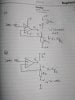
DAC controlled from a microcontroller fed into the non inverting input of an opamp. The opamp has split supplies +/-5V. The out put of the opamp drives the gare of a n channel MOSFET. The drain is at 0V and the source is connected to a 100K resistor then to the load. The resistor at the source is fed back into the inverting feedback pin of the opamp. The idea being that whatever the DAC input is will be seen at the feedback pin, so I equals DAC/R.
Will this circuit work. I have the drain more positive than the source (which I think will be negative) or do I need to use a p channel MOSFET?
Any help will be appreciated.
Thanks,
Rajinder
 

(*steve*)

¡sǝpodᴉʇuɐ ǝɥʇ ɹɐǝɥd
Moderator
Jan 21, 2010
25,510
Joined
Jan 21, 2010
Messages
25,510
can you draw the schematic and upload it? It will be a lot easier to make sure we have the same thing in mind.

In general, if you compare the voltage drop across a resistor with the output of a DAC and use this to control a pass element you'll get a programmable current source/sink.
 

AnalogKid

Jun 10, 2015
2,893
Joined
Jun 10, 2015
Messages
2,893
Your verbal description of the circuit is very incomplete. For example, where does the other end of the load go? If GND, the circuit will not work.

ak
 

Rajinder

Jan 30, 2016
568
Joined
Jan 30, 2016
Messages
568
can you draw the schematic and upload it? It will be a lot easier to make sure we have the same thing in mind.

In general, if you compare the voltage drop across a resistor with the output of a DAC and use this to control a pass element you'll get a programmable current source/sink.
Hi,
Yes this is what I am doing. But I need to get a negative current output. Hence the drain to 0V and the output of my source to the load. I will upload a schematic in a few minutes. Thanks. Rajinder.
 

Rajinder

Jan 30, 2016
568
Joined
Jan 30, 2016
Messages
568
Your verbal description of the circuit is very incomplete. For example, where does the other end of the load go? If GND, the circuit will not work.

ak
Hi, I will upload a schematic in a few minutes. Thanks for your reply. I need to get this to work, do would appreciate any help. Best regards, Rajinder.
 

Rajinder

Jan 30, 2016
568
Joined
Jan 30, 2016
Messages
568
Hi,
Yes this is what I am doing. But I need to get a negative current output. Hence the drain to 0V and the output of my source to the load. I will upload a schematic in a few minutes. Thanks. Rajinder.
Hi
Here is the schematics. The first one works but I can't get a common ground between the load and the unit that it needs to connect too. Hence the second circuit idea, which gives the common ground but I can't get the negative current output. Can I connect the n channel FET drain to 0v and source to output negative voltage. Or will a P channel FET work. Look forward to hearing from you. Best regards, Rajinder
 

Attachments

  • IMG_20160131_100059039.jpg
    IMG_20160131_100059039.jpg
    113 KB · Views: 259

(*steve*)

¡sǝpodᴉʇuɐ ǝɥʇ ɹɐǝɥd
Moderator
Jan 21, 2010
25,510
Joined
Jan 21, 2010
Messages
25,510
if your DAC produces a positive voltage wrt ground then you can use an inverting amplifier (gain = -1) to make it negative wrt to ground then place your current sense resistor between gnd and the mosfet.
 

Rajinder

Jan 30, 2016
568
Joined
Jan 30, 2016
Messages
568
if your DAC produces a positive voltage wrt ground then you can use an inverting amplifier (gain = -1) to make it negative wrt to ground then place your current sense resistor between gnd and the mosfet.
Hi,
I have done this. With an inverting gain of -1 using 2 x 10 M resistors. Non inverting tied to 0v, DAC fed to inverting input stage, I removed the FET band placed resistor across the opamp output wrt ground. This works fine. But is open loop with no feedback control. I was looking at some feedback for better control hence FET and feedback loop.
Is there anyway that I could get it working with the FET configurations?.
Best regards, Rajinder.
 

Rajinder

Jan 30, 2016
568
Joined
Jan 30, 2016
Messages
568
Your verbal description of the circuit is very incomplete. For example, where does the other end of the load go? If GND, the circuit will not work.

ak
Hi,
My idea was to have the drain of the FET go 0V, gate driven by opamp and the source providing the negative voltage. Will this configuration work? The output is taken from drain (as I need a common 0V) and the source end which has the feedback resistor to the opamp inverting pin. I look forward to hearing from you.
Best regards, Rajinder
 

(*steve*)

¡sǝpodᴉʇuɐ ǝɥʇ ɹɐǝɥd
Moderator
Jan 21, 2010
25,510
Joined
Jan 21, 2010
Messages
25,510
the inverting amplifier gives you the voltage reference, you use another opamp to compare this voltage with the voltage across the sense resistor while the output drives a mosfet to control the current.
 

Rajinder

Jan 30, 2016
568
Joined
Jan 30, 2016
Messages
568
the inverting amplifier gives you the voltage reference, you use another opamp to compare this voltage with the voltage across the sense resistor while the output drives a mosfet to control the current.
Hi,
Thanks for your help so far. Do you have a sketch if the circuit? What I understand is, that I have my current set up I.e. inverting opamp gain of -1, non inverting input at 0V. DAC connected to inverting input, so what ever is at the DAC output is seen at the opamp output but negative voltage. Are you saying that I apply this negative input to the input of another opamp (non inverting input). Which drives the gate of my n channel FET and sense resistor fed back to my inverting input still connected to the source? Drain connected to +Vdd? I would appreciate some clarification on this second opamp connection or a schematic/sketch of the complete circuit. Will this give me a negative current and common 0V between units? I look forward to hearing from you. Best regards, Rajinder
 

(*steve*)

¡sǝpodᴉʇuɐ ǝɥʇ ɹɐǝɥd
Moderator
Jan 21, 2010
25,510
Joined
Jan 21, 2010
Messages
25,510
ill try to draw a schematic
 

(*steve*)

¡sǝpodᴉʇuɐ ǝɥʇ ɹɐǝɥd
Moderator
Jan 21, 2010
25,510
Joined
Jan 21, 2010
Messages
25,510
Sorry about the delay.

This is sorta what you need.

negisource.png

R1 = R2. Note that the impedance of Vin (from your DAC) should have an impedance X << R1.

R4 helps stop U2 from oscillating. A value of a 10Ω should be sufficient.

R3 is the current sense resistor. The voltage across R3 will equal -Vin when the circuit is regulating the current.

Note that R1 = R2 is not strictly necessary. You may wish to have a gain less than -1 (like -0.5) so that the voltage drop across R3 can be smaller.

The point labelled -Vin is there just to label the voltage at this point (it is actually -Vin * R2 / R1)
 

(*steve*)

¡sǝpodᴉʇuɐ ǝɥʇ ɹɐǝɥd
Moderator
Jan 21, 2010
25,510
Joined
Jan 21, 2010
Messages
25,510
The above circuit can be simplified somewhat.

negisource2.png

The calculations in this circuit are the same, however rather than the current output being (Vin * R2) / (R1 * R3) it is (Vin * R2) / (R1 * R3) - (Vin / R1) or ((Vin * R2) - (Vin * R3)) / (R1 * R3)

This can be trimmed out either in the gain of the stage (R2 / R1) or by making allowances in the DAC or the value fed to it. (or it can be ignored if R2 >>> R3 -- which it normally is)
 

Rajinder

Jan 30, 2016
568
Joined
Jan 30, 2016
Messages
568
The above circuit can be simplified somewhat.

View attachment 24764

The calculations in this circuit are the same, however rather than the current output being (Vin * R2) / (R1 * R3) it is (Vin * R2) / (R1 * R3) - (Vin / R1) or ((Vin * R2) - (Vin * R3)) / (R1 * R3)

This can be trimmed out either in the gain of the stage (R2 / R1) or by making allowances in the DAC or the value fed to it. (or it can be ignored if R2 >>> R3 -- which it normally is)
Hi Steve,
Thanks for your help. I will give this a go today and let you know of the outcome. I really appreciate you taking time out to help. Best regards, Rajinder
 

Rajinder

Jan 30, 2016
568
Joined
Jan 30, 2016
Messages
568
H
Hi Steve,
Thanks for your help. I will give this a go today and let you know of the outcome. I really appreciate you taking time out to help. Best regards, Rajinder
Hi Steve,
Many thanks for your help. The circuit works as expected. Thank you again for your help. Best regards, Rajinder
 

Rajinder

Jan 30, 2016
568
Joined
Jan 30, 2016
Messages
568
The above circuit can be simplified somewhat.

View attachment 24764

The calculations in this circuit are the same, however rather than the current output being (Vin * R2) / (R1 * R3) it is (Vin * R2) / (R1 * R3) - (Vin / R1) or ((Vin * R2) - (Vin * R3)) / (R1 * R3)

This can be trimmed out either in the gain of the stage (R2 / R1) or by making allowances in the DAC or the value fed to it. (or it can be ignored if R2 >>> R3 -- which it normally is)
Hi Steve,
Thanks for all your help with this problem
I wanted to ask something. My understanding of the n channelosfet for this design is that Drain voltage must be greater than source voltage. Also gate voltage must be greater than vgs threshold. So am I correct in saying that because the drain is at 0V (more positive than the negative on the source) this is why this configuration is working. Also as long as we have a vgs greater than threshold it works. Does this put the fet into saturation region? Look forward to hearing from you. Best regards, Rajinder
 

Rajinder

Jan 30, 2016
568
Joined
Jan 30, 2016
Messages
568
Hi Steve,
Thanks for all your help with this problem
I wanted to ask something. My understanding of the n channelosfet for this design is that Drain voltage must be greater than source voltage. Also gate voltage must be greater than vgs threshold. So am I correct in saying that because the drain is at 0V (more positive than the negative on the source) this is why this configuration is working. Also as long as we have a vgs greater than threshold it works. Does this put the fet into saturation region? Look forward to hearing from you. Best regards, Rajinder
I have wired the circuit with a n channel, drain to 0V, sense resistor taken from source and voltage feedback from this to inverting input of opamp. You have a P channel FET. I am not sure why my circuit is working correctly? Any ideas?
Best regards, Rajinder.
 

(*steve*)

¡sǝpodᴉʇuɐ ǝɥʇ ɹɐǝɥd
Moderator
Jan 21, 2010
25,510
Joined
Jan 21, 2010
Messages
25,510
Sorry, you have wisely used an N channel MOSFET. I must have pulled a P channel symbol by mistake.
 
Top