Maker Pro
Maker Pro

unbiased portion of transistor

chet

Nov 15, 2016
12
Joined
Nov 15, 2016
Messages
12
I have a circuit where the designer has connected the collector of one transistor directly to the base of a second transistor. There is no biasing on this connection. The remaining two points on each transistor are tied to voltages. How do you evaluate the voltage and current in this unbiased collector to base connection?
 

davenn

Moderator
Sep 5, 2009
14,260
Joined
Sep 5, 2009
Messages
14,260
I have a circuit where the designer has connected the collector of one transistor directly to the base of a second transistor. There is no biasing on this connection. The remaining two points on each transistor are tied to voltages. How do you evaluate the voltage and current in this unbiased collector to base connection?


Hi
welcome :)

can you show an example or 2 just so we all know what you are referring to and specially so that it shows what other components may be influencing the design


Dave
 

73's de Edd

Aug 21, 2015
3,622
Joined
Aug 21, 2015
Messages
3,622
Sir chet . . . . .

Is there a possibility that you have just encountered your first encounter with a darlington connected pair of transistors.Its used to get some phenomenal gain possibilities.
The first depiction is the Darlington and the second is a variance to the circuit to tailor the gain characteristics down somewhat, if you are getting more gain than you actually wanted.
That is by using the collector load and mainly, the added R-shunt resistor.
" GOGGLE " up Darlington if you need more info . . . .saving me some keystrokes.

An then, there is the " Suuuuuuuper " transistor pair . . . NOW . . .being known as a " Sziklai pair ",
look that one up also.

73's de Edd
 
Last edited by a moderator:

chet

Nov 15, 2016
12
Joined
Nov 15, 2016
Messages
12
Charger.JPG

Here is the circuit diagram. My exposure to the Darlington has all points biased.
The N1, N2, and N3 are 2N5551, P1 & P4 are 2N5401 and P2 & P3 are 2N4403, R is a 431.
 
Last edited by a moderator:

73's de Edd

Aug 21, 2015
3,622
Joined
Aug 21, 2015
Messages
3,622
Sir chet . . . .

Is there a strong possibility that you have one of these and it is inoperative ?
Looks like one other person had this situation and he also plotted up a schematic.
I copied his and reversed the right to left positioning of what he drew up as a 3 terminal regulator.
It now shows up as a better and now properly positioned 431 programmable zener.
Check out his drawing and see which of you are correct in comparing against a unit.
It has your parts values transferred onto it .

CIRCUIT DESIGN wise, I am seeing two transistors configured as a unijunction transistor, it being used for variable drive to the gate of the SCR, yet another set of transistors sample and modify the switching rate of the unijunction pair in accordance to the initial RAW dc voltage output.
A set on the other side sample the regulated output of the 431 and further correct the drive to the SCR.
A final voltage threshold pair, feed back a correction voltage to the gate of the SCR.

Looks like SEVERAL of these units have failed on customers.

ROUGH DRAFT :

Initial_rough_draft_Chicago_66783_Chgr.png


73's de Edd


Last edited by a moderator:

chet

Nov 15, 2016
12
Joined
Nov 15, 2016
Messages
12
Sir chet . . . .

Is there a strong possibility that you have one of these and it is inoperative ?
Looks like one other person had this situation and he also plotted up a schematic.
I copied his and reversed the right to left positioning of what he drew up as a 3 terminal regulator.
It now shows up as a better and now properly positioned 431 programmable zener.
Check out his drawing and see which of you are correct in comparing against a unit.
It has your parts values transferred onto it .

CIRCUIT DESIGN wise, I am seeing two transistors configured as a unijunction transistor, it being used for variable drive to the gate of the SCR, yet another set of transistors sample and modify the switching rate of the unijunction pair in accordance to the initial RAW dc voltage output.
A set on the other side sample the regulated output of the 431 and further correct the drive to the SCR.
A final voltage threshold pair, feed back a correction voltage to the gate of the SCR.

Looks like SEVERAL of these units have failed on customers.

ROUGH DRAFT :

Initial_rough_draft_Chicago_66783_Chgr.png


73's de Edd

Thanks for your input. Not sure this circuit ever worked. I have used the start mode several times but the start switch bypasses the SCR. Every time I tried to use in the charge mode, the green light came on with no current flow even with a dead battery. Your sketch says it is the Chicago electric 66783 which is the unit I have.
 
Last edited by a moderator:

chet

Nov 15, 2016
12
Joined
Nov 15, 2016
Messages
12
Sir chet . . . .

Is there a strong possibility that you have one of these and it is inoperative ?
Looks like one other person had this situation and he also plotted up a schematic.
I copied his and reversed the right to left positioning of what he drew up as a 3 terminal regulator.
It now shows up as a better and now properly positioned 431 programmable zener.
Check out his drawing and see which of you are correct in comparing against a unit.
It has your parts values transferred onto it .

CIRCUIT DESIGN wise, I am seeing two transistors configured as a unijunction transistor, it being used for variable drive to the gate of the SCR, yet another set of transistors sample and modify the switching rate of the unijunction pair in accordance to the initial RAW dc voltage output.
A set on the other side sample the regulated output of the 431 and further correct the drive to the SCR.
A final voltage threshold pair, feed back a correction voltage to the gate of the SCR.

Looks like SEVERAL of these units have failed on customers.

ROUGH DRAFT :

Initial_rough_draft_Chicago_66783_Chgr.png


73's de Edd

Dear Sir, Some of what you say goes over my head. How might I evaluate what you call a uni junction transistor in terms of voltage and current.? Thanks
 

chet

Nov 15, 2016
12
Joined
Nov 15, 2016
Messages
12
Dear Sir, Some of what you say goes over my head. How might I evaluate what you call a uni junction transistor in terms of voltage and current.? Thanks
Another interesting thing is the SCR which is an S6055K, when I did a diode check between the gate and the cathode of the original I got roughly 0.325 volts in either direction, that is it did not matter whether I connected the positive to gate or cathode. So I ordered a new one from China, it measures 0.025 volts in either direction between gate and cathode. I expected something like 0.235 volts in one direction and OL in the other.
 

73's de Edd

Aug 21, 2015
3,622
Joined
Aug 21, 2015
Messages
3,622
I was just about to quiz you about the SCR that the unit used so I would know its gate sensitivity.
Now you mention [an original] being involved, and I perceive of your having a new one in your hand
now.
The new China one extremely suggests of being BAAAAAD.
If it so happens that you still have BOTH I can give you a dynamic test that will only involve having a load for the
charger like an automotive incandescent tail light lamp or borrow Mamma Cass's clothes pressing iron,
which will also need 2 clip leads for its inteconnects.
Also a 470 ohm resistor or two 1 K units.
Have you confirmed the other schematic to your units components and their values and wiring runs ?
BUT the non triggerable SCR may be the units sole problem.

73's de Edd
 

chet

Nov 15, 2016
12
Joined
Nov 15, 2016
Messages
12
Again thanks for your reply. The schematic you sent me looks very much like mine. Did I understand you correctly that you transferred my component values to the schematic you sent me? Do you know what the "shopstop" on the schematic refers to? You say the new SCR is bad but what about the original? Would you expect the gate to cathode diode check to be the same regardless of reversing positive and negative leads? What kind of gate voltage would trigger either the SCR or the 431 zener? I guess I am very anal but I still would like to understand the physics if possible of the direct connection between the collector of one trans to base of another. I will set up the test you suggest. Thanks again.
 

chet

Nov 15, 2016
12
Joined
Nov 15, 2016
Messages
12
I just noticed you are in Texas. We just moved back to PA after spending 20 some years in Texas, Beaumont and then Houston.
 

chet

Nov 15, 2016
12
Joined
Nov 15, 2016
Messages
12
So here is the latest, I used an ohm meter set at X1000, with positive connected to anode and negative to cathode, infinite resistance. I touch the positive lead to gate, resistance goes to zero, remove the positive lead to gate and resistance goes to infinity. This is the behavior of both old and new scr. The behavior described in the literature says once the voltage applied to the gate is removed, the scr should continue to conduct. not so here.
 

chet

Nov 15, 2016
12
Joined
Nov 15, 2016
Messages
12
Just for grins I put the new SCR on the board and hooked everything up to my car battery. I plugged it in on charge and the amps went to 7 amps and stayed for about 30 seconds, the green light came on and the amps dropped to zero. My car battery was not low to begin with. So it appears that it works but there may be an issue if the battery is severely discharged and the voltage is too low to trigger. So this SCR appears to be like no other in terms of its characteristics and I still do not understand how these unijunction transistors work. Two of the combinations go from a "P"collector to a "P" base junction and one goes from an "N" collector to a "P"base junction if that means anything.
 

duke37

Jan 9, 2011
5,364
Joined
Jan 9, 2011
Messages
5,364
#12 " the scr should continue to conduct. not so here."

The scr will only continue to conduct if it is passing more than a minimal holding current.
 

73's de Edd

Aug 21, 2015
3,622
Joined
Aug 21, 2015
Messages
3,622
Sir chet . . . . . .

I was busy transferring the resistor values from your schema to the other one that I had found and was then just basically consulting his schema on that made observation.
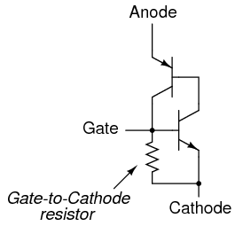
Its common design fare to use either a digital stream or a simpler single unijunction transistor to drive a SCR 's gate.
Since unijunctions are becoming in less favor after a 50 year design / use period. Prices are going up on them.greatly.
It is possible to cheaply replicate them with a single cheeeeep NPN and PNP transistor pair.
Your made up schema is providing better referencing to the left of the schema, so I now refer to your copy and see that actually, no " simulated " unijunction transistor function was being replicated by the use of a cross coupled NPN and PNP transistor.
I do see a variant of the Sziklai pair being used with N1 and P4 transistors.
That pair is being used to get a high gain of a voltage sampled at the output of the 431 programmable zener diode reference, over to the base of N3 which is being used to variably trim in the drive level being fed into the gate of the SCR.

Since you did not mention if you had initially tested all of the transistors for having good C to B and B to C junctions, lets now try some tests on your fully wired up unit.

You said that your hook up to your car battery gave a quite short charge time before the activation of the GREEN LED.
You can avert that by either the turning on and leaving of the headlights on HIGH beam and the activation of the fresh air moving car ventilation system in HIGH motor / fan position.
Leave them on for a time period to drag down your battery charge state a bit, or also leave them on during testing.
We just want to be able to see that ammeter pointer . . . being between scale limits . . . and see the charge current variances.

Take a double clip ended test wire and one clip lead end goes to the base of N3 and then you observe the charge ammeter reading and place the free clip end lead to any of the common ground buss points at the bottom of the schematic.
Which direction did the ammeter pointer then swing, and if any effect on the GREEN LED intensity . . .if being on ?
Move the double clip ended test wire and have one clip lead end to the base of P1 and make the same initial observation of the ammeter and then the same grounding of the free clip.
Here, we are also equally interested in the ammeters pointer direction .

My final interim info here, is for your query of:

Do you know what the "shopstop" on the schematic refers to?

That is the definition that he self assigned to the auto reset/overload circuit breaker which you correctly show on your schematic.
Its likely to pop . . .and very s.l.o.w.l.y. cycle, if you happen to use the high current START mode for too long.

Thasssssit


FOR TECHNO REFERENCING:

Chicago_Electric_66783_Barr_Chgr.jpg


Chicago_Electric_66783_Internals.jpg


73 ' s de Edd
 
Last edited by a moderator:

chet

Nov 15, 2016
12
Joined
Nov 15, 2016
Messages
12
Just ran the test with the car headlights on high beam. The current went to 13 amps and stayed. I finally turned of the headlights and the needle very gradually moved from the 13 amps down toward 7 amps. When it reached 7 amps the green light came on and amps dropped to zero. Seems to be working as it should.
 

chet

Nov 15, 2016
12
Joined
Nov 15, 2016
Messages
12
Thanks for pointing out the Sziklai transistor arrangement. I had never heard of this before. There are similarities. In the Sziklai the unbiased line goes from an "N" base of one transistor to an "N" collector of the other transistor. In our schematic. We have a "P" base going of one transistor going into a "P" collector of the other transistor. I am starting to think these function by a saturated base of one transistor spilling over into a like kind collector of another transistor.
 

chet

Nov 15, 2016
12
Joined
Nov 15, 2016
Messages
12
The SCR must be one on those that places a resistor between the gate and the cathode so the diode check will only show the resistor in both directions.
03324.png

Replacing the SCR has solved the problem with the battery charger. if the auto feature ever stops working, you can by pass the SCR by switching from charge to the start position. It is to be noted thou that the connectors for the battery will be hot and not voltage isolated as in the charge position.
 
Top