PCB designing is an intricate process requiring technical expertise in terms of both designing and material sourcing
PCB designing is an intricate process requiring technical expertise in terms of both designing and material sourcing. A lot of newbies get into the field of PCB designing with little to no experience and end up wasting a lot of time on simple designs that cost them significantly. Pursuing guidance in terms of best implementable standards for PCB designing and assembly is not something only newbies struggle with. A lot of PCB fabricators also strive to determine the best ways, standards & disciplines that they can implement an order to maximize their production yield. So, in today’s article, we are going to go over the top five golden rules of PCB designing and manufacturing that will help you in saving both time and money in your next PCB designing project.
op 5 Golden Rules For Saving Time & Money In PCB Manufacturing
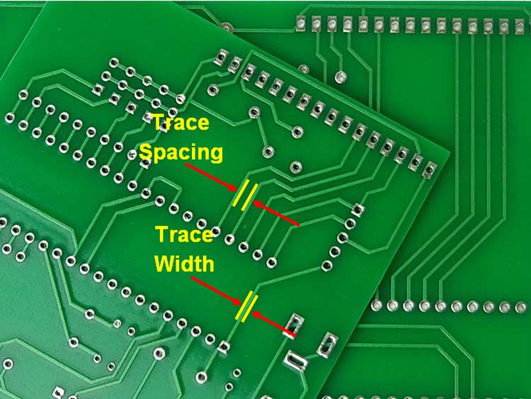
1) Be Mindful of Traces and Spacing
copper traces are buses that join one PCB part to another part or to vias (holes plated with copper). It is basically a wire for your connections. Generally a width trace of 0.005” is a good minimum trace width but 0.007” or 0.008” would help ensure that the manufacturing process produces a high-quality board. While a trace width smaller than 0.005” is possible. the extra care, processes, and restrictions required can result in higher costs. The same is true of spacing. A minimum of 0.005” of space between copper traces, or between copper traces and other features like holes and ground planes, will allow for efficient manufacturing. Spacing greater than 0.005” will help prevent instances of copper features “shorting out”.
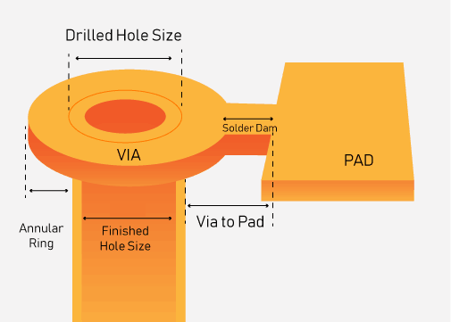
2) Always Make Sure That A Solid Connection Between the Pad & Hole exists
Always Make Sure That A Solid Connection Between the Pad & Hole exists. The purpose of the pad is to ensure that the copper plated in the hole makes a solid connection to the traces that are connected to the pad. Ideally, the pad size should be at least 0.015″ larger than the hole size. For instance, if you have a finished hole size of 0.010″ then the final size of the pad for that hole would be 0.025″
3) Hole Sizes are Crucial
The hole size and how the holes will be connected to traces in the design is integral for the success of your PCB. The ability to drill smaller holes has increased greatly in the last decade. Today, it is standard to be able to have a finished hole size of 0.010″ but of course, if you can use 0.015″ or 0.020″ the process and quality will be much easier to maintain.
4) Provide Adequate Spacing between the Copper & the edge of Your PCB
Another key rule is related to the spacing from copper to the edge of the board. Ideally, any copper used in your design should be no closer than 0.010” to the edge of the board. Any closer than 0.010” will increase the risk of copper being exposed after the board has been routed.
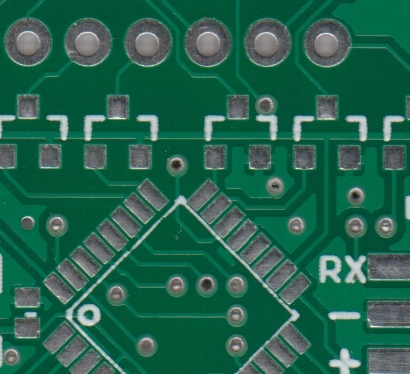
 Closeup detailed shot of a printed circuit board
5) Quality Soldermask & Silkscreen
Always make sure that your designs have a quality layering of solder mask covering the pads. Bad solder masks can end up in undesirable design errors, prolonging your design & costing you unnecessarily. Also, be mindful about putting all the necessary labels and info into the top silkscreen of the PCB. This small detail will help you in avoiding any last-minute design discrepancies and will help you in saving time and money in the long run as well.