Binary adders come in two types: Half Adders and Full Adders. A half adder adds 2-bit binary numbers but cannot include a carry bit. In contrast, a Full Adder adds the carry bit along with the two binary numbers, enabling the addition of multi-bit binary numbers by cascading multiple Full Adder circuits.
Full Adder Circuit
The main limitation of a half adder is the lack of a ‘Carry in’ bit. In a Full Adder circuit, we include a carry in input and add it to inputs A and B, giving us three inputs (A, B, and Carry In) and producing two outputs (SUM and Carry Out).
Full Adder Block Diagram
The Full Adder is constructed by combining two half-adder circuits and an OR gate. Here’s how it works:
- The first half-adder adds inputs A and B, producing SUM and Carry out.
- The SUM output from the first half-adder is fed into the second half-adder along with the Carry in bit.
- The final SUM output is the result of the Full Adder.
- The Carry out bits from both half-adders are combined using an OR gate to produce the final Carry out.

Construction of Full Adder Circuit
Here’s a step-by-step guide to constructing a Full Adder Circuit:
Components Needed
- Two Half Adder circuits
- OR Gate
- Steps
- Connect the inputs A and B to the first half-adder.
The SUM output from the first half-adder goes to the input of the second half-adder along with the Carry in bit.
The final SUM output from the second half-adder is the overall SUM output of the Full Adder.
Combine the Carry out bits from both half-adders using an OR gate to produce the final Carry out.
Circuit Diagram and Logic Gates
The full adder circuit utilizes XOR, AND, and OR gates. The two half adders are connected such that the first half adder handles inputs A and B, while its SUM output and the Carry in bit are fed into the second half adder. The OR gate then combines the Carry out bits from both half adders.
Truth Table of Full Adder Circuit
The truth table for the Full Adder circuit includes three inputs (A, B, Carry In) and two outputs (SUM, Carry Out):

The SUM output is obtained by XORing inputs A and B and then XORing the result with the Carry in bit. The Carry out is calculated by ORing the AND results of the input pairs.
Practical Demonstration: Full Adder Using IC 74LS283N
To demonstrate a practical Full Adder, we use the IC 74LS283N, a 4-bit full adder with carry look-ahead features. Here’s a list of components required:
- 74LS283N IC
- 4-pin DIP switches (2 pcs)
- Red LEDs (4 pcs)
- Green LED (1 pc)
- 4.7k resistors (8 pcs)
- 1k resistors (5 pcs)
- Breadboard
- Connecting wires
- 5V adapter
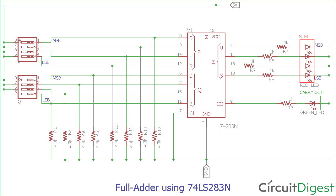
Circuit Setup
Connect the VCC and Ground to pins 16 and 8, respectively.
Connect the first 4-bit number to pins 5, 3, 14, and 12 (P inputs).
Connect the second 4-bit number to pins 6, 2, 15, and 11.
The SUM outputs will be on pins 4, 1, 13, and 10.
Use 4.7k resistors on all input pins to set logic 0 when switches are off.
Use red LEDs for SUM outputs and a green LED for the Carry out bit.
For a visual demonstration, check out the video tutorial below where we show adding two 4-bit binary numbers using the 74LS283N IC.
Understanding Full Adder circuits is crucial for digital electronics. By combining half adders and using logic gates, we can build efficient circuits for adding binary numbers, with applications ranging from simple calculators to complex computer systems.
Watch the detailed video tutorial here: Full Adder Circuit Tutorial.