Graphene nanoribbons hold plenty of promise thanks to their electrical properties and tiny stature. Measuring in at only a single carbon atom’s thickness and featuring high conductivity, some of their theoretical applications wouldn’t seem out of place in science fiction. This theory, however, lays far ahead of reality, with current graphene nanoribbons falling far short of their potential.
Now, a new collaborative study, from the Nara Institute of Science and Technology (NAIST) and other researchers such as those from Fujitsu and the University of Tokyo, has reported the first ever 17-carbon-wide graphene nanoribbon. The researchers claim that it has the smallest bandgap seen to date when compared with other graphene nanoribbons.
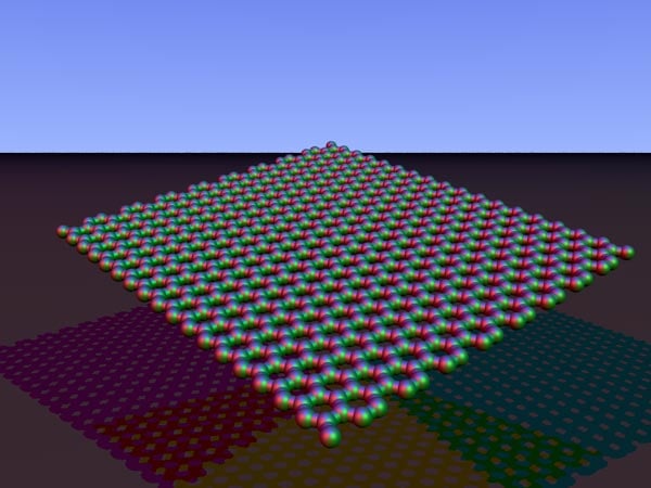
A diagram of the atomic structure of a carbon nanoribbon. Image Credit: Wikimedia Commons.
The NAIST team’s research was published in Communications Materials on the 23rd of June.
‘Bottom-up’ Synthesis
Electronic devices, such as smartphones and laptops, are now a ubiquitous part of our lives, and it is large-scale integrated circuits (LSICs), which use silicon semiconductors in such devices, that enable their function. And although LSICs have improved device performance by a magnitude we could never have foreseen (while simultaneously miniaturising them), LSIC miniaturisation is quickly approaching its limit due to Moore’s Law. And at a time when pressure from consumers for smaller and more powerful devices is always increasing, this is not ideal.
According to the research team, however, their graphene nanoribbons, which were synthesised using a ‘bottom-up’ process, could come to the rescue. Said Dr Shintaro Sato of Fujitsu Ltd: “Silicon semiconductors are giving us better performance at smaller sizes. However, we are reaching the limit in how small we can make devices. Thus, we have high expectations for the performance of graphene nanoribbons, which have semi-conducting properties that are only one atom thick—a 2D material.” Sato also says that new methods and/or materials are needed to solve the challenges that face further miniaturisation.
Graphene Nanoribbons
The nanoribbons have similar honeycomb-like structures to their more popular and widely known cousins, namely carbon and graphene nanotubes. However, graphene nanoribbons feature unique electronic and magnetic properties that cannot be found in two-dimensional graphene. “Interestingly, the electronic and magnetic properties of graphene nanoribbons are widely tuned as a function of the width and edge structure,” says Professor Hiroko Yamada at NAIST.

A diagram of the atomic structure of an ‘armchair’ carbon nanoribbon. Image Credit: Wikimedia Commons.
Armchair-type graphene nanoribbons, a promising type of nanoribbon for electronic devices, display a width-dependent bandgap. The NAIST researchers explain that they can be classified into three subfamilies—namely ‘3p’, ‘3p + 1’, and ‘3p + 2’ (‘p’ stands for a natural number)—and their bandgaps are inversely proportional to the width of those families. Simply put, the wider armchair-edge graphene nanoribbons belonging to the 3p + 2 subfamily have the smallest bandgaps among different graphene nanoribbons and hold significant potential for nanoribbon-based devices.
To date, 13-armchair bandgap nanoribbons of the 3p + 1 subfamily (with a bandgap of more than 1 electron volt) have been reported, but the research team’s work shows the synthesis of a 17-carbon nanoribbon belonging to the 3p + 2 subfamily, which have even smaller bandgaps.
Synthesis of the graphene nanoribbons was based on the ‘on-surface synthesis’ method, also known as the said ‘bottom-up’ method. “There are many methods to synthesise graphene nanoribbons, but to produce atomically precise graphene nanoribbons, we decided to use the bottom-up approach,” said Dr Hironobu Hayashi.
The team expects their 17-carbon-wide graphene nanoribbons to provide the foundations for new graphene nanoribbon-based electronic devices.
