What is a 3D-IC?
A 3D-IC, or three-dimensional integrated circuit, is a chip that accommodates two or more layers of active electronic components, which are integrated vertically as well as horizontally. Each active layer contains functional units, such as sensors, micro-electrical mechanical systems (aka MEMS), analogue RF circuits, processor cores, and memory arrays.
How 3D ICs are Structured
Through-silicon-vias (TSVs), which are copper vias with diameters ranging from 1 to 30 um, are inserted in the 3D-IC to deliver power/signal/ground among the different tiers, as well as to facilitate communication between the various devices within each of the different layers.
These TSVs pierce the underlying silicon substrate to connect the circuitry on different layers, and they enable the integration of multiple stacked dies. Usually, the diameter of the TSVs, the number and density of these TSVs, and the thickness of the layers determine the performance of the finished 3D-IC.
Why 3D Integration?
Unlike traditional 2D layout implementation, the stacking of regular 2D chips to achieve 3D integration is effective in improving the inter-chip bandwidth, resulting in the faster exchange of data—which, in turn, enhances the performance of the system. 3D integration can also result in increased integration densities, the co-integration of heterogeneous components, and overall system energy savings.
This technology is well-suited for high-performance ASICs (application-specific integrated circuits). Its early implementation was in CMOS (complementary metal oxide semiconductors) image sensors, where the image sensor is stacked over the logic that is responsible for data processing.

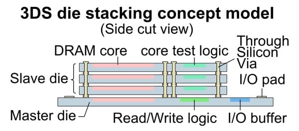
A diagram to illustrate the 3DS die stacking concept model. Image Credit: Wikimedia Commons.
The Major Challenges
As promising as 3D-IC may now sound, there are still challenges that need to be addressed before a 3D-IC can bring integration, cost, and performance benefits. Using a TSV, for example, poses integration challenges relating to design, thermodynamics, test, and mechanical stress.
Design Challenges
Conventional design tools are geared towards 2D technology, and when a design engineer introduces 3D, it means there is an extra control variable that needs to be factored into the design process.
In addition, every die must be designed for stacking, and this requires a considerable design effort. Close collaboration is especially required when various entities are responsible for the different layers. The designers need to understand what’s on each chip, how they are connected, the timing delays, and so on. These requirements increase the complexity of figuring out the design dynamics of the chips.
Thermal Challenges
Having several layers of electronic components stacked together means there is going to be a higher power density compared to traditional 2D-ICs. This causes potential thermal issues. The middle layers that don’t require heat may be unable to expel the unnecessary heat, resulting in a significant thermal challenge.
The work of the design team, therefore, is to establish the thermal modelling required for the dies to interact so that they don’t melt. 3D-IC designers are tasked with finding new, efficient ways of dissipating the heat produced by internal dies and avoiding hot spots.
Testing Challenges
Chips need to be tested before packaging, of course; however, the structure of 3D-ICs poses a challenge because the middle dies are not easily accessible, and thinned wafers need proper handling. The solution, accordingly, is to have an architecture that provides efficient ways to control and observe each die from the chip I/Os. Therefore, the test access for a 3D stack requires considerable pre-planning.
Mechanical Stress Challenges
As a result of the use of TSVs and the size of the corresponding die, 3D-ICs are exposed to challenges relating to mechanical stress.
The die needs to be thin enough, given that there is a limit to the length of TSVs that can be fabricated reliably. TSVs induce thermal-mechanical stress, as a result of a thermal expansion mismatch between the chosen TSV-filling material (various options apply) and silicon. The thermal stress results in potential reliability problems, such as cracking.
Because some dies have TSV that goes through them—and, again, TSV induces stress—designers must figure out how to design 3D-ICs to minimise (or even avoid) stress. Mechanical stress can significantly alter transistor performance.
All in all, as long as Moore’s law continues to be a dominant path for digital ICs, the industry will find ways of solving the above problems (at least until Moore’s law becomes economically and/or technically-infeasible). Indeed, the industry may well rise to the said challenges, and 3D-ICs will likely become mainstream.With that said, for now, maybe 2.5D (aka ‘interposer technology’) could be a viable compromise; after all, it has a way around the aforementioned shortcomings of 3D integration. In fact, adopting 2.5D means designers can buy the time needed to work out some of the challenges—and ultimately build all the more confidence and experience in stacking technologies.