What is Graphene?
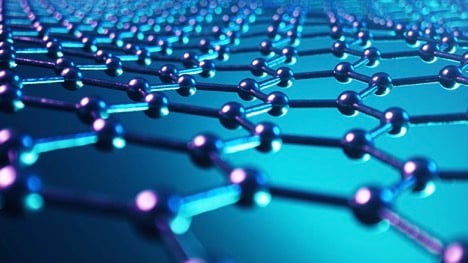
Graphene is a two-dimensional, single-layer lattice of carbon atoms and it is the building block for other graphitic materials. A single millimetre of graphite has around three million layers of graphene.
Discovered by Konstantin Novoselov and Andre Geim back in 2004, graphene belongs to a new class of materials called two-dimensional (2D) materials.
Features
This 'wonder material' is the strongest material known to man.
Graphene is more elastic than rubber, lighter than aluminium (1 square metre weighs around 0.77mg), and tougher than diamond and steel (between 100 to 300 times stronger than structural steel with the same density and tensile strength). But that’s not all; graphene has other remarkable traits:

Sketch of graphene material features. Image courtesy of SketchWork.
Graphene is one of the most promising nanomaterials. Its spectacular properties make it suitable for a wide range of applications ranging from biodevices and electronics to sensors and optics. It is also one of the most investigated materials today that may replace a material like silicon.
However, despite the multitude of astonishing properties, this supermaterial is still expensive to produce in large quantities, and this has limited its use in products that are mass produced. Don’t expect to see graphene being utilised in consumer products quite yet.
Silicene
Silicene, the silicon equivalent of graphene, is the thinnest possible two-dimensional form of silicon. It is an allotrope of silicon, the same way graphene is an allotrope of carbon, and is composed only of silicon atoms (monoatomic). Unlike other 2D materials like graphene, silicene is not strictly planar: it has a buckled honeycomb surface—atoms are arranged above and below the main 'panel,' which creates a band gap.
Silicene’s first structures were observed on silver crystal, and they had a hexagonal form like graphene, though not entirely flat. In joint research between the University of Aix Marseille and the Technical University of Berlin, researchers created isolated silicene by condensing silicon vapour on silver.

Scanning tunneling microscope photographs of silicene growth. Image courtesy of Wikimedia Commons.
Compared to other 2D materials, silicene is not widely studied nor produced because it is much harder to create than a 2D material like graphene: its 3D form is a diamond-like lattice.
Silicene must be synthesised from the beginning and cannot be 'pulled out' of a stack of tightly held 2D layers like graphene can: silicon tends to form three-dimensional structures, and a 2D form of silicon will often buckle. Therefore, silicene cannot be produced through exfoliation, but only through epitaxial growth.
Since 2012, silicene monolayers have been synthesised on different kinds of substrate surfaces including iridium, silver, and molybdenum disulfide.
Silicene vs Graphene
-
Unlike graphene, silicene does not depend highly on pi-electrons and, as a result, is not reliant on pi-stacking mechanisms.
-
Silicene is not entirely planar. It has a hexagonal pattern of atoms like graphene, but these hexagonal rings have puckering distortions as a result of its “chair” configuration.
-
Silicene has a bandgap that makes it suitable for use in novel transistors. Graphene, on the other hand, is a semi-metal and does not have any bandgap.
-
Silicene is more convenient to integrate into electronic devices when compared to graphene, especially for smaller and cheaper electronic devices. This is because it can be easily integrated into silicon chip production lines.
Features
-
By adding hydrogen in an exothermic reaction, silicene can be converted to silicane.
-
Its electronic properties are similar to those of graphene; it shares the so-called Dirac electronic dispersion observed in it.
-
It is sturdy like graphene and can be used in the anodes of lithium-ion batteries. Silicene would offer twice the capacity for the anode, and its strength would prevent it from undergoing changes during charging and discharging.
-
Silicene has stronger spin-orbit coupling that can lead to quantum spin Hall effect at temperatures attainable in experiments.
For the longest time, silicene was limited to speculation. However, density functional theory (DFT) calculations performed back in 2011 indicated that silicene will be suitable for FET (field effect transistor) applications. Its energy band gap can be much finer tuned, enabling a field effect transistor to operate better at room temperature. In fact, the possibility of tuning the 2D Dirac points implies that silicene can be used alongside existing silicon technology because of novel properties, mainly the various quantum spin effects.
Due to its buckled honeycomb lattice structure that favours spin-related actions, silicene is a suitable material for ferromagnetism. Silicene spintronics is a vast research area with potential applications in areas such as spin filter, spin FET, and gas sensor. However, silicene has high reactivity, which puts a limit to its uses and also makes it harder to create free-standing silicene sheets. In most instances, silicene will exist stacked with alternating metal monolayers or as part of a substrate layer.

Photograph of a microscopic view of plumbene. Image courtesy of Nagoya University.
Plumbene
Plumbene is a 2D-honeycomb sheet of lead atoms and, just like silicene, it has a buckled honeycomb structure and a large band gap (−400 meV).
Researchers from Nagoya University, led by Professor Junji Yuhara, finally synthesised this once purely theoretical lead-based two-dimensional honeycomb material—their study was originally published (in early May) in the Journal of Advanced Materials.
Plumbene is Graphene’s newest cousin–it has a similar structure and could have a wide range of applications for topological insulators. In past research aimed at investigating plumbene’s electronic structure and topological properties, researchers found that plumbene, through electron doping, can become a topological insulator with a large bandgap (−200 meV).
Differences
-
Plumbene should exhibit the Quantum Spin Hall Effect, and this is possible even above room temperature. This is not achievable with a 2D material like graphene. Therefore, finding a cheap and reliable way of synthesising Plumbene is crucial.
-
Among the Group 14 elemental 2D materials, Plumbene has the largest spin-orbit interaction. This makes it a robust two-dimensional topological insulator.
How Was Plumbene Created?
Plumbene was created by annealing a super thin lead on palladium. Annealing is a method of heating and slowly cooling a substance to remove internal stresses. A scanning tunnelling microscopy (STM) revealed that, by annealing, the researchers came up with a surface material that had the distinct honeycomb structure of a two-dimensional monolayer.
During this experiment, the researchers found a surprising by-product: a palladium-lead (Pd-Pb) alloy film which had a structure that resembled the complex 3-dimensional Weaire-Phelan structure devised by Denis Weaire in 1993. The Weaire-Phelan structure helps to solve the 'Kevin Problem', and it inspired the 'Water Cube' used for the Beijing Olympics in 2008.
Why is it a Big Deal?
Plumbene, besides being a 2D material like graphene and silicene, has had heads turning because it’s ideal as a topological insulator, and has the largest spin-orbit interaction among the three, as well as the largest bandgap. This makes Plumbene a robust 2D topological insulator in which the Quantum Spin Hall Effect might occur.
Plumbene could revolutionise the development of topological insulators. According to Yuhara, the arrival of Plumbene is good news, and it should trigger a scramble for application development involving it.