What Are the Benefits of 3D Printing?
The main benefit of 3D printing for electrical and electronics systems design is the reduction of costs and time of prototyping. Prototyping printed circuit boards isn’t cheap, after all: it often requires multiple versions of a board, which can get expensive as manufacturers have minimum order requirements. This leaves engineers paying for multiple PCB copies that they will never use.
Additionally, engineers sometimes take the cheaper route by ordering prototypes from Asian manufacturers. This reduces the cost of manufacturing, but it drastically increases the time it takes for the prototype in question to reach its engineer. Lead times can range from one week to even a matter of months.
With 3D printing, however, these times can be cut from weeks to hours if carried out in-house, which enables rapid prototyping, quick redesigns, and—with that—a higher quality end product. Furthermore, the price per prototype drops as only one board is printed at a time.

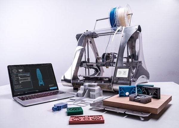
An assortment of 3D printing technologies, including additive manufacturing design software on a laptop. Image Credit: Pixabay.
3D Printing for Electronic Systems Design
3D printing circuit boards don’t end at the prototype stage, moreover, as such technology also offers the use of multiple extruders (an extruder is the part that heats up and pushes out the given filament) as well as various types of filaments.
Working with dual extruders allows users to print both conductive and non-conductive material on the same layer at the same time—thus making it possible to create either an encapsulated or product-embedded PCB. As this technology matures, we’re bound to see PCBs that take the shape of complex three-dimensional objects.
Moreover, having a three-dimensional space to freely layer both conductive and non-conductive material makes it possible to 3D print electronic components, such as resistors, capacitors, and inductors. These components can be printed either individually or as modules within one package—essentially meaning the user can print the whole circuit, not just the board. An example of this would involve designing a sensor and then 3D printing the whole electronic system as one object, all in one go.
An addition to these technologies are flexible filaments that can produce a flexible 3D printed object. Flexible filaments open up a multitude of possibilities in the area of wearable tech. They facilitate the creation of flexible instruments, such as sensors and custom-made medical devices that can be embedded in clothing, applied to the skin, or even under the skin.
Given all the advancements in this technology, these types of 3D-printed devices could eventually become the norm in the future.

A 3D printer connected to a laptop. Image Credit: Thomas Quine via Flickr.
3D Printing for Electrical Systems Design
Aside from the said benefits that this technology can bring to electronic systems design, but it is of great value to electrical systems design as well.
Because the technology grants its users the ability to print conductive and non-conductive materials on the same layer, it enables the printing of wires within the very structural components of a device. This means that, instead of designing two detachable parts that need to be attached with wiring in-between them, an engineer could print one already-wired part that does that exact same function. Not only can this process save time and eliminate errors, but it could potentially make both a more structurally sound and much more lightweight product.
Furthermore, this technology opens up the possibility of embedding parts—like switches, antennas, and even induction coils (for integrating charging and communication capabilities within the product that is being designed). An example of this would involve printing an enclosure for an RFID circuit that has the induction coil, the power switch, and the battery holder—all already built in.
While such a feature is still experimental, the potential for growth is nevertheless vast as 3D printing technology advances: it has the potential to alter many of the current ways in which consumer electronics is being designed and produced.

Consider what the future has in store for 3D printing. Pictured: an additive manufacturing machine from the International Space Station that printed the first 3D-printed object in space. Image Credit: NASA.
The Future of 3D Printing in the Field
Currently, this 3D printing technology is in its early stages and it’s not ready for wide use. But the progress made in this field in the past couple of years by industry leaders and STEM university departments suggest that it’s bound to pick up more traction as 3D printer resolution improves and the development of both more robust non-conductive materials and less resistive conductive materials.
Indeed, as companies are adopting 3D printing as a tool for the design and development of electronic and electrical systems, we’re very likely to see consumer electronics produced—particularly if the technology of interest hits the market within the next couple of years.