For example, SiC-based semiconductors have been used in devices that use Schottky barrier diodes (SBD), as well as hybrid inverters that likewise have SBD, plus silicon insulated gate bipolar transistors (IGBT).
Now comes the newest advancement of SiC epitaxial wafers, developed by Showa Denko (aka SDK, a Japan-based manufacturer of chemicals and petrochemicals): introducing the second-generation high-grade SiC epitaxial wafer (HGE-2G), which can be used in power semiconductors to improve reliability and produce large chips at scale.
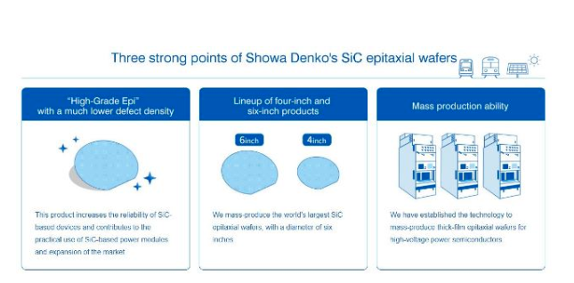
Next-gen Epitaxial Wafers with 150 mm Diameters
SDK recently announced that it has further improved its said HGE (or ‘High-Grade Epi’, to use SDK’s exact trade name of the technology) model. This is by applying a new technology that enables the manufacture of modules with 6-inch (150 mm) diameters, suitable for the mass production of high-voltage power semiconductors.
Historically, the company has been known to work on enhancing its use of CVD, aka chemical vapour deposition (links to MIT’s definition) equipment. CVD can be applied to the production of SiC epitaxial wafers in a variety of sizes, and SDK is one of the manufacturers that have succeeded in putting the metal-oxide-semiconductor field-effect transistor (MOSFET) into practical use.
Lower Surface Defect Density < 0.1 cm²
In order to be efficient in their mass production of large chips (10 mm²), SDK managed to keep the surface defect (SD) density of the new HGE-2G model under 0.1/cm².
Specifically, it’s due to such SD limitations in the HGE-2G SiC epi-wafer modules that improvements have been made in the epitaxial growth process and energy loss has been minimised.
In fact—said enhancements to the controlled defect density has resulted in the new model being half the size of its original HGE predecessor, which will even potentially help power device manufacturers to come up with smaller electronic components still.
The reliability improvement is also a result of the increased basal plane dislocation (BPD) conversion rate, which is 10 times larger than that of the first HGE.
A 3-part infographic that shows the major improvements in Showa Denko’s second-generation high-grade silicon carbide (SiC) epitaxial wafers (collectively named HGE-2G). Image courtesy of Showa Denko Japan.
In consideration of their ability to perform under extreme conditions, including high temperatures, high current, and high radiation, the hybrid SiC semiconductors are already in use in data centre servers, as well as in dispersion-type power modules for the expansion of power supply sources to renewables—including solar power, inverter modules for railcars, and battery chargers for electric vehicles (EVs).
Solving the Cost-Performance Ratio Problem
The cost-performance ratio of SiC wafers has long been recognised as a common problem for the mass industrial application of large-sized chips in high-performance devices.
Despite the higher productivity, increasing wafer size has been met with reluctance from many manufacturers in the past—naturally because of the massive price tag that accompanied larger diameters. Now, however, the improved thermal conductivity that comes with the HGE-2G’s said high temperature efficiency, allows engineers to work with new product designs at scale and improve the otherwise-problematic cost-performance ratio.
Apart from such improved reliability, the cost-effective innovation by SDK also offers a new solution to other typical industry problems, such as energy-saving and system integration.
The market prognosis for SiC epitaxial wafers is altogether promising. The demand for this product is going to further increase in the next 5 years, especially with the need for more highly efficient and sustainable EVs. The same goes for the utilisation of renewables—especially solar power—which is predicted to double in size by 2025.
Ultimately, the technology’s said advantages altogether mark a significant step for SDK to solidify its position as one of the leading manufacturers of SiC semiconductors and modules.