Since then, transistor technology has progressed rapidly, with advancements in semiconductor manufacturing allowing engineers to build increasingly powerful devices while minimizing power consumption. In this article, we’ll explore the many benefits of low power design for electronic applications.
Power Consumption in Low-power Devices
Portable modern devices such as mobile phones, notebook computers, and smartwatches contain ICs that provide functionality in the device. These chips consist of millions of transistors that contain logical gates that control the behavior of electric circuits.
Electric power dissipated in a transistor can be dynamic; as often as the transistor gates change in value, or static; as a result of leakage current. Dynamic power loss increases as the number of gates and operating frequency increases, while static power loss increases with shrinking process geometry.
Static Power Dissipation
Is expressed in a diode as the product of the leakage current and supply voltage: PS = Leakage current x Supply voltage.
Dynamic Power Dissipation
Is expressed in a diode as the sum of the transient power dissipation and capacitive-load power dissipation: PD = PT + PL
(Where PD = Dynamic power dissipation, PT = Transient power dissipation, and PL = Capacitive-load power dissipation)
Benefits of Low-Power Design
Engineers utilize a variety of low-power design techniques to minimize power consumption in electronic devices. But first, let’s take a look at some advantages of low-power design:
Energy Savings
An obvious benefit of designing for low-power is that devices utilize less power than high-power or high-voltage systems. Power electronics such as bipolar junction transistors (BJTs) and metal–oxide–semiconductor field-effect transistors (MOSFETs) integrated into modern low-power devices have smaller power losses (conduction and switching losses) than high-voltage systems resulting in additional power savings.
Efficiency
Low-power design generates minimal heat, which reduces the overall power consumption and improves efficiency. In modern semiconductors, chip architects use a mix of AI, Machine Learning, and Deep Learning techniques to optimize the efficiency of microprocessors at the wafer-level. Billions of these chips integrated into portable devices such as smartphones, tablets, laptops, and wearables produce devices that run efficiently and at lower temperatures.
Reliability
At lower voltages, solid-state components tend to fail less frequently. One reason for this is that low-power operation prevents overcurrent conditions and the consequent overheating which can cause damage to sensitive electronics. Also, when components work within their specified operating temperatures, the device requires less-frequent maintenance.
Miniaturization
A significant benefit of low-power design in the modern age is that engineers can design increasingly compact devices without sacrificing efficiency. Low-power applications utilize portable energy storage devices such as supercapacitors or Li-ion batteries which come in multiple sizes and capacities with high power solutions available in compact footprints. These batteries can be charged using portable solar panels attached to the body of the device.
Moreover, low-power electronics are often designed to be modular or have several functions embedded in a single chip. Besides allowing designers to meet space constraints, it also saves power since the greater the number of components, the higher the power consumption.
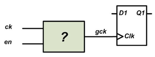
Clock gating to reduce the power consumption of a CMOS transistor. Image courtesy of All About Circuits.
Challenges of Low-Power Design
As transistors shrink in size to sub-micron (< 10-nanometer) levels, leakage power dissipation emerges as the most prominent challenge. The leakage power dissipation is due to leakage current in the transistor which is inversely proportional to the size of the circuit. In CMOS transistors, leakage power can occur in both the conducting and non-conducting states. Hence, the most effective low-power techniques at this level are those aimed at minimizing power loss.
Engineers can use these techniques to minimize power consumption in technology nodes:
Power Gating
Power gating is an IC design technique that helps to conserve power by shutting off the current to sections of the chip that are not in use. It uses PMOS transistors with low leakage currents to shut off the power supply to parts of the IC that is in idle or sleep mode. Power gating is one of the most effective techniques for reducing leakage power in low-power electronics.
Clock Gating
Clock gating is a low-power design technique for minimizing dynamic power dissipation. It conserves power by “masking” the clock signal in logic cells having no activity. Gating the clocks helps prevent switching losses in the combination logic and flip-flops. All About Circuits explains how clock gating reduces dynamic power dissipation in this article.
Frequency and Voltage Scaling
Dynamic voltage scaling is a technique used to conserve power in portable electronics such as smartphones and laptops that utilize power from an energy source with limited capacity such as a battery.
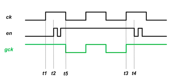
Clock gating an asynchronous circuit. Image courtesy of All About Circuits.
During normal operation, MOSFET-based circuits use voltages at the nodes to represent logical states. Switching to a lower voltage mode coupled with low clock frequency helps reduce power consumption in CPUs when lower performance is preferable. Conversely, the system switches to higher voltages and frequencies when there is justifiable demand for greater computational power. The continuous toggling between states helps conserve power.
As we’ve discussed, there are significant benefits that justify designing electronics that use less electric power. Clock gating, power gating, and frequency and voltage scaling are some of the most effective techniques for optimizing the efficiency of low-power systems while minimizing power consumption.