Thanks to their small size, they have largely aided the miniaturisation of electronic devices and equipment. This article looks at the past and present of such vital technology.
A Brief History of the IC
In Washington DC, 1952, a British electronics engineer named Geoffrey Dummer became the first person to conceptualise an integrated circuit. However, he was unable to translate his ideas into a working model. (Meanwhile, several other scientists from around the world, such as Yasuro Tarui and Sidney Darlington, had also suggested the design of a single board that contains several transistors.)
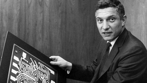
It was only until mid-1958 that the first practical IC was demonstrated by Jack Kilby, an engineer working at Texas Instruments. While working on a solution for the ‘tyranny of numbers’—namely a problem that states the need to have a large number of discrete modules to increase the complexity of electronic circuits—Jack realised that the solution to such an issue was to integrate all the electronic components into a single piece of semiconductor material.
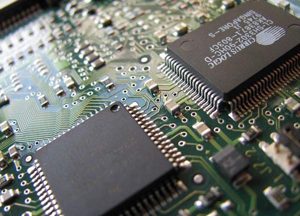
A close-up of two integrated circuits and surface-mount capacitors on a printed circuit board.
Early IC Designs
Kilby’s design of the world’s first practical IC model was adopted four years later by the U.S. Airforce. Such a device was a hybrid IC that had components linked with physical wires on a germanium substrate. And while this meant that it could only be produced in limited quantities, Kilby nevertheless earned the 2000 Nobel prize in Physics for his groundbreaking invention.
In 1959, Robert Noyce, a physicist working at Fairchild Semiconductors, designed what came to be known as the first monolithic IC. Rather than using wires, Noyce connected all the components on a silicon substrate with copper traces. This design revolutionised semiconductor manufacturing in terms of cost, performance, and size, ultimately allowing manufacturers to integrate increasing numbers of components on a single chip. Notably, two processes—namely surface and planar passivation—enabled the production of true monolithic ICs, which we will discuss shortly.
Surface Passivation and Planar Processes
Surface passivation is a technique developed in 1958 by Mohamed Atalla of Bell Telephone Labs. It involves coating a semiconductor substrate or base wafer with a thin layer of silicon dioxide via thermal oxidation. Surface passivation helps to shield the surface of ICs from corrosion due to environmental factors such as moisture.
Following Atalla’s work on surface passivation, the planar process was developed in 1959 by Jean Hoerni, an engineer working at Fairchild Semiconductors. The basic concept remains to implement IC design on a 2-dimensional plane using photographic processing techniques. The planar process involves the following:
-
Forming a layer of silicon on the substrate to preserve its semiconductor properties
-
Etching the substrate to create contact points for transistors
-
Depositing metal layers onto the substrate to connect the various components

An example of a metal-oxide-semiconductor field-effect transistor. Image Credit: SparkFun Electronics, Flickr.
Modern IC Design
Metal-oxide-semiconductor field-effect transistors, or MOSFETs (example pictured above) have been utilised in IC designs since the early 1960s and are still in full swing today. However, the most notable difference is in the significantly higher volumes of components that are currently being integrated into silicon substrates: using advanced manufacturing techniques, several billions of transistors can be fitted into a silicon chip roughly the size of a human fingernail.
Naturally, this has led to an explosion in the speed and processing capabilities of the computerised systems that utilise these components.
3-dimensional integrated circuit (3D-IC) design allows several wafers to be stacked on top of each other and connected with special connectors (such as through-silicon vias, or TSVs), altogether enabling all the layers to perform a unified function.
In fact, such technology also allows manufacturers to design chips with higher performance, lower power consumption, and smaller footprints. (Consider IBM in 2015, for instance, which has already launched its 7-nanometre computer chips that contain transistors having widths about the size of a strand of human hair.)
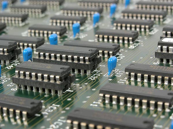
A close-up of a multitude of integrated circuits, all mounted on a computer circuit board.
Applications
Integrated circuits are found in virtually every kind of electronic device today. Some of the most crucial applications are covered in the next five sections.
Computers
Most famously of course, ICs are commonly utilised in computer processors: computer chips hold millions or billions of transistors are responsible for carrying out numerous computations (namely instructions per second) from within a central processing unit, or CPU.
Amplifiers and Oscillators
Another common application of ICs is in the amplifier and oscillator circuits of electronic devices and equipment. In amplifiers, ICs harness the capabilities of transistors to increase the amplitude of input signals, such as frequency, voltage, current, and power. Whereas in low-frequency, audio, and radiofrequency oscillators, they are used to convert direct current into alternating current.
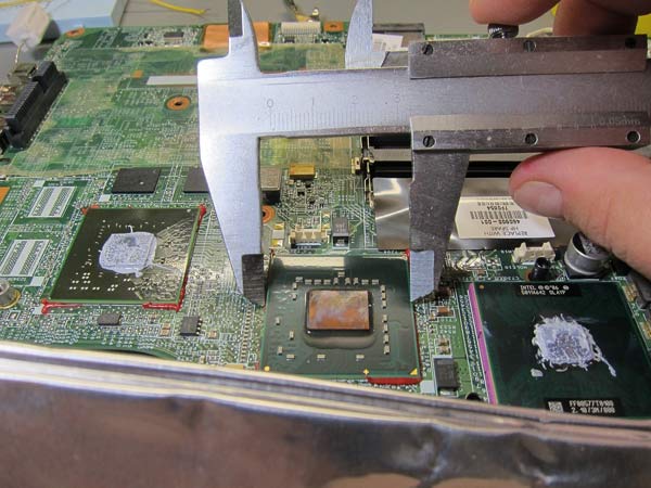
An engineer’s first-person view as they use a caliper to measure an integrated circuit (mounted on a laptop’s circuit board).
Military Systems
ICs are employed in a wide range of defence and surveillance systems, such as drones, armoured vehicles, sonar systems, and radar systems. Electronic circuits that contain computer chips are used to process, analyse, encrypt, and store information for various military divisions and agencies.
Aerospace Systems
ICs are also ubiquitous components in the communications, controls, and location systems of aeroplanes and helicopters. In manned and unmanned spacecraft, computerised systems obtain and process data about space and relay the information back to ground control stations.
Taking Stock of the Importance of IC Design
Considering the points above, it’s all the more clear why the invention of the integrated circuit in the 20th century was one of the most impactful moments in the history of electrical engineering. Indeed, to this day, ICs continue to shape the technological world—thanks to their miniature size, performance, low-power consumption, and much more.