The VU19P is a big FPGA, to say the least; a 35 billion transistor device that has been described as "the world's largest" by its developer, Xilinx. Whilst it is small when compared to other more advanced chips, for example, AI chips, it is huge for a traditional chip or FPGA.
The VU19P's Main Features
Featuring 9 million system logic cells, the 16nm VU19P is nothing short of a monster. It delivers "the highest logic density… device ever built" thanks to its incorporation of 35 billion transistors.
The chip also has up to 1.5 terabits per-second of DDR4 memory bandwidth, up to 4.5 terabits per-second of transceiver bandwidth, and more than 2,000 user I/Os. It is 1.6X larger than its predecessor, the 20nm Virtex UltraScale 440 FPGA, that had been the industry's largest FPGA until now, on which engineers can simulate 10 concurrent Arm Cortex A9 cores. On the new VU19P, engineers can simulate 16 of these thanks to the 1.6X increase in logic gates.
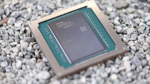
The VU19P. Image courtesy of Xilinx.
“This is our third generation of world-record FPGAs. First was the Virtex-7 2000T, followed by the Virtex UltraScale VU440, and now the Virtex UltraScale+ VU19P. But this is more than silicon technology; we’re providing robust and proven tool flows and IP to support it" said Sumit Shah, Xilinx Senior Director of Product Line Marketing and Management. He added, "The VU19P enables developers to accelerate hardware validation and begin software integration before their ASIC or SoC is available…"
Built upon TSMC's 16FF+ process, the VU19P is built in four segments before being placed on a die to act as a single, seamless chip.
What's Its Purpose?
The 16nm VU19P is designed for ASIC and SoC creators that use FPGAs for emulation and prototyping. The FPGA enables developers to begin software integration before the silicon becomes available.
In their announcement, Xilinx explained that a huge part of their business is providing hardware to the simulation and emulation market and that the constant drive towards bigger chips compelled them to act and create the VU19P.
As readers may well know, an FPGA, or Field Programmable Gate Array, is hardware that enables circuit designers to design and deploy an integrated circuit before it goes to market. This allows engineers to see if their design works and whether its performance and accuracy are viable for its intended function.
Some of the VU19P's other applications include aerospace and defence, test, measurement, and networking.
About Xilinx
Founded in 1984 and headquartered in San Jose, California, Xilinx, Inc., is an American technology company. Primarily, Xilinx develops and supplies programmable logic devices such as FPGAs and CPLDs, the former of which the company invented. It is also the company that created the first fabless manufacturing model.
This year, Xilinx exceeded $3 billion in annual revenues for the first time, up 24% from the previous financial year.
