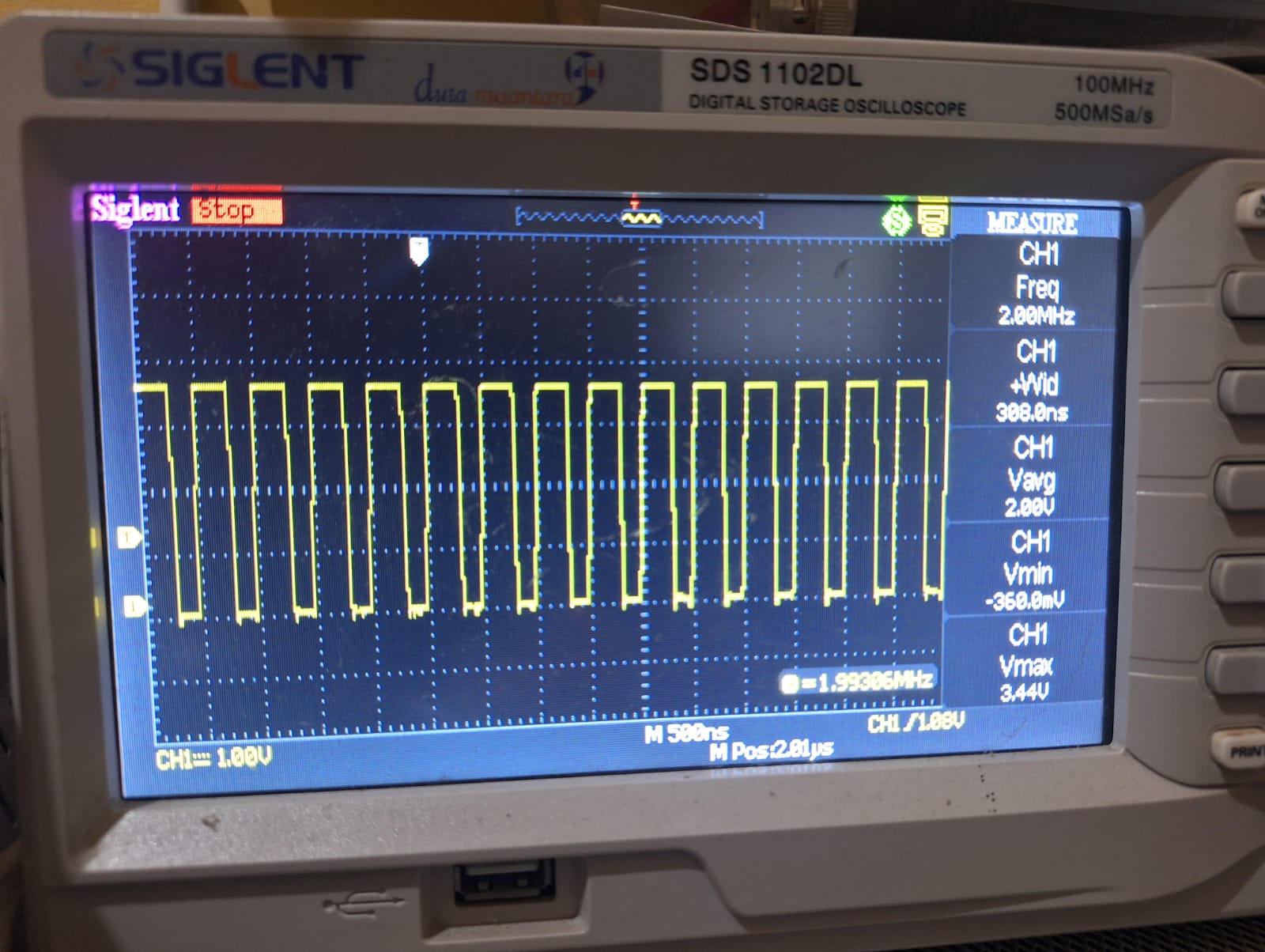
This project uses the PIC16F13145’s onboard Configurable Logic Block (CLB) to generate a 2 MHz pulse width modulation (PWM) waveform with 4 bit duty cycle resolution (16 levels)—entirely in hardware, with zero CPU intervention once configured. The result is a high-speed, low-jitter PWM source ideal for applications ranging from LED drivers to high-
What It Does & Why It’s Cool
2 MHz PWM Carrier
Pushes beyond typical microcontroller PWM limits (often <1 MHz) to drive high-speed power stages or generate high-frequency analog waveforms.
4‑Bit Duty Resolution
Offers 16 discrete duty‑cycle steps (0 – 93.75 %), enough for coarse modulation without overwhelming hardware.
Hardware‑Only Implementation
All counting, comparison, and output toggling occur inside the CLB fabric. The CPU is free to perform other tasks (sensors, communications, control loops).
Minimal Jitter & Latency
CLB logic operates synchronously at the device’s fastest clock speed (up to 32 MHz), yielding clean edges and predictable timing, which is critical for precision applications.
Detailed Operation Flow
CLB Counter Loop
A small chain of flip-flops and LUTs creates a 4-bit modulo‑16 counter clocked at the full CLB clock rate.
Threshold Compare
A second LUT continuously compares the current count against a configurable duty value (0–15).
Output Toggle
When the count is below the threshold, the CLB outputs 0 to the PWM. Otherwise, it produces the desired duty cycle.
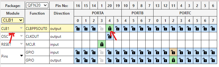
PPS Routing
The resulting PWM signal is mapped to any GPIO pin using the Peripheral Pin Select (PPS) system, making integration into your hardware effortless.
How to Reproduce
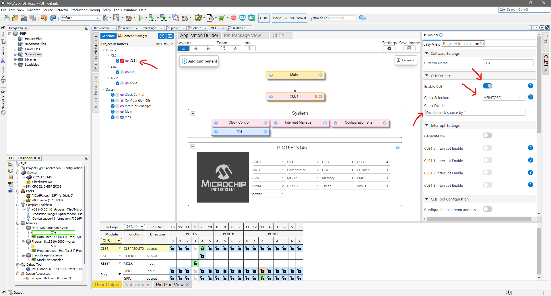
Set Up MCC
Enable CLB1 and assign CLB clock to HFINTOSC (32 MHz).
Clock Divider set by 1
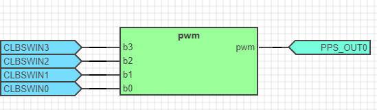
Design in CLB Synthesizer
Add a 4-bit counter (flip‑flops + LUT feedback).
Add a LUT configured as a “less‑than” comparator against a 4-bit input port (your duty value).
Connect the comparator output to a CLB output port.
module pwm(CLK, b3, b2, b1, b0, pwm);
input CLK, b3, b2, b1, b0;
output reg pwm;
reg [3:0] counter;

    always @(posedge CLK) begin
        counter <= counter + 1'b1;
        if(counter > {b3,b2,b1,b0})begin
            pwm <= 1'b1;
        end else begin
            pwm <= 1'b0;;
        end
    end

endmodule
add input and output port like this figure
Design in CLB Synthesizer
Add New Verilog module, give "pwm" name and use this code
add inputs and output ports similar to this figure
#include "mcc_generated_files/system/system.h"

/*
    Main application
*/

int main(void)
{   uint8_t data = 0;
    SYSTEM_Initialize();
    // If using interrupts in PIC18 High/Low Priority Mode you need to enable the Global High and Low Interrupts
    // If using interrupts in PIC Mid-Range Compatibility Mode you need to enable the Global and Peripheral Interrupts
    // Use the following macros to:

    // Enable the Global Interrupts
    //INTERRUPT_GlobalInterruptEnable();

    // Disable the Global Interrupts
    //INTERRUPT_GlobalInterruptDisable();

    // Enable the Peripheral Interrupts
    //INTERRUPT_PeripheralInterruptEnable();

    // Disable the Peripheral Interrupts
    //INTERRUPT_PeripheralInterruptDisable();
    while(1)
    {
        CLB1_SWIN_Write8(data);
        __delay_ms(100);
        data++;
        if(data > 15)
            data = 0;
    }
}
Demos Video
How the CLB Transformed the Design
Entirely Autonomous: The CLB fabric loops and compares at hardware speed—no interrupts or timer overhead.
Pin-Selectable Output: PPS allows you to assign PWM to any available pin without requiring code changes.
Ultra‑Low Latency: Edges occur on the very next CLB clock cycle, ensuring minimal phase error.
Scalable: By trading off count width and compare logic, you can boost resolution or frequency as needed.