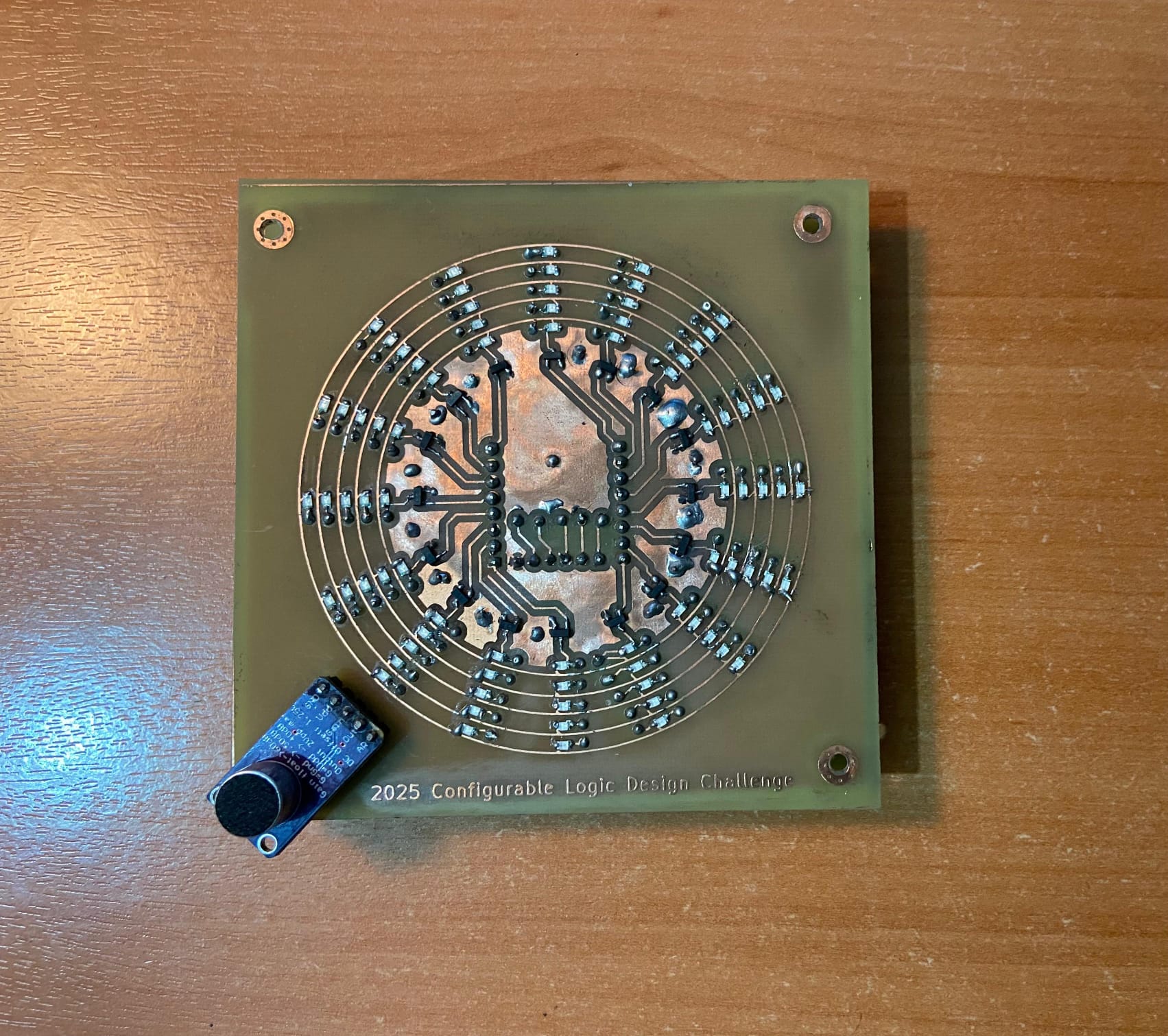
CLB Accelerated Circular FFT Audio Spectrum Visualizer captures audio via a microphone, performs FFT, and displays the spectrum on a circular LED matrix. CLB handles both row and column control with only one interrupt, enabling smooth real-time visualization with minimal MCU resource usage.
1. Introduction
In this project, a real-time audio visualization system is implemented using a resource-constrained microcontroller. The system captures sound signals through an analog microphone, performs a Fast Fourier Transform (FFT) to analyze the frequency components, and displays the results on a custom LED matrix.
Unlike traditional solutions that rely heavily on software processing or external hardware accelerators, this design offloads most of the display logic to the Configurable Logic Block (CLB) of the microcontroller. Using only a single interrupt and minimal CPU intervention, both column and row control of the LED matrix are handled directly in logic, significantly reducing the processing overhead.
The communication between the software and the CLB is established through the CLBSWIN register, which transmits bar height and column index data. Additionally, a special startup animation is rendered using logic-based LED control (Mode 0), and the system then transitions to FFT-based bar mode (Mode 1) for live audio visualization.
This approach enables a low-latency, low-power, and highly responsive visual output suitable for embedded spectrum analyzers, VU meters, or interactive music-driven displays.
2. System Overview
Audio Sampling
The system captures incoming audio signals via an analog microphone connected to the microcontroller’s ADC. Sampling is performed at a frequency of 32 kHz, providing sufficient resolution to analyze audio content up to 16 kHz in the frequency domain. Each sample is stored in a buffer until the required number of samples (64) is collected.
Fast Fourier Transform (FFT)
Once the buffer is full, a Fast Fourier Transform (FFT) is performed on the collected samples. This converts the time-domain signal into its frequency-domain representation, exposing the signal's spectral components. Only the magnitude of the output is used for visualization.
Data Filtering and Normalization
The FFT output is first passed through a square-root stage to obtain the true magnitude, then normalized to a 0–5 scale, matching the vertical resolution of the LED matrix. An optional low-pass filtering stage smooths rapid changes, enhancing the visual stability and reducing noise-induced flickering.
CLB Communication
After processing, the resulting 5-bit bar height data is packaged with the current column index and mode flag, and written to the CLBSWIN register.
CLBSWINM (upper byte) contains the 4-bit column index and 1-bit mode selection.CLBSWINL (lower byte) contains the 5-bit bar height.
This compact structure enables high-speed data transfer to the CLB using minimal MCU resources.
LED Matrix Control
The Configurable Logic Block (CLB) controls both row selection and column data shifting entirely in hardware. Every 1 ms, one column is updated by sending a new value to the CLB, which manages shift register clocks, data pulses, and row activation signals internally. This eliminates the need for constant CPU intervention.
Startup Animation
Before entering active FFT mode (mode = 1), a startup animation is executed using mode = 0. In this state, the CLB displays a visually engaging boot sequence using predefined bar patterns, shifting them across the LED matrix in timed steps.
Timing and Interrupt Handling
Two hardware timers synchronize the system:
- Timer1 triggers ADC sampling at 32 kHz, ensuring consistent and accurate audio acquisition.
- Timer2 generates an interrupt every 1 ms, responsible for column-wise updates to the CLB.
All operations are interrupt-driven, ensuring non-blocking execution, low CPU usage, and smooth real-time performance.
The hardware architecture integrates standard modules and custom logic to achieve efficient audio visualization.
Microcontroller and CLB
At the heart of the system lies a microcontroller equipped with an integrated Configurable Logic Block (CLB). The CLB handles the hardware control of the LED matrix, managing row and column scanning signals autonomously, which significantly reduces CPU workload. The microcontroller's firmware writes display data into the CLBSWIN registers, interfacing seamlessly with the CLB.
Microphone Module and ADC
The audio input is provided by a ready-made analog microphone module connected to the microcontroller's ADC input pin. The module includes necessary amplification and biasing circuitry, simplifying hardware design and improving signal quality. The ADC samples the microphone output at 32 kHz to capture the audio waveform accurately.
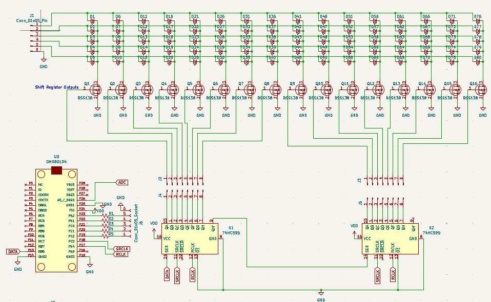
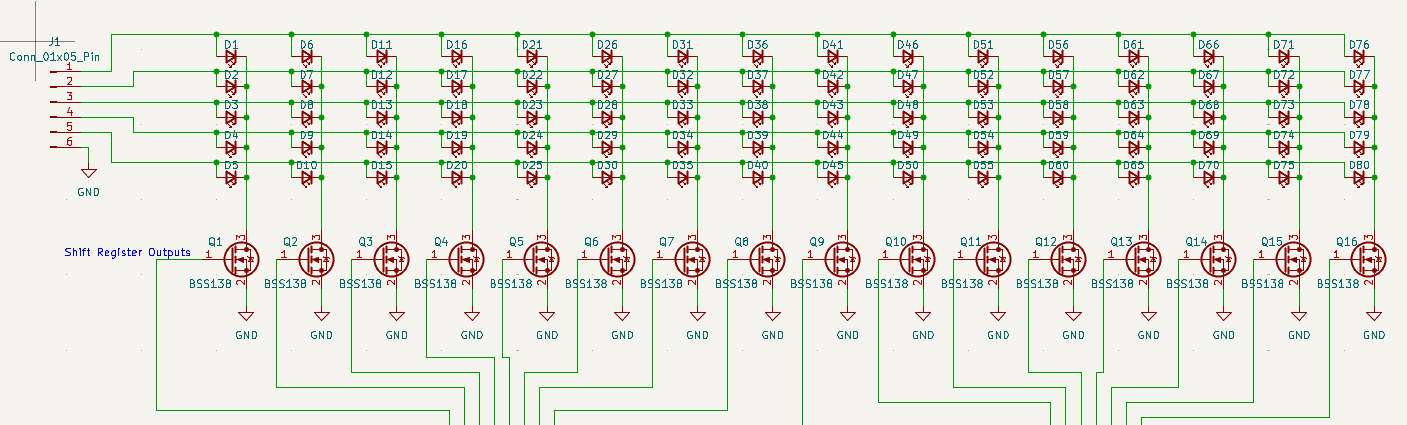
LED Matrix and Driver Circuitry
The visual output is presented on a custom 16-column by 5-row LED matrix. The CLB controls the multiplexing of rows and columns through dedicated output pins and possibly external shift registers such as the 74HC595 for column driving or level shifting. MOSFETs like BSS138 may be incorporated in the switching circuitry to handle voltage requirements or improve signal integrity.
3. CLB Design
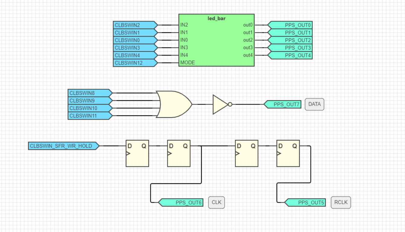
Mode-Dependent LED Output Logic Module
Verilog module that drives 5 LED outputs based on 5 input bits and a mode selector. In Mode 0, each input is directly mapped to its corresponding output. In Mode 1, a logic-based bar graph pattern is generated using only combinational logic, providing a simple VU meter-like visualization.
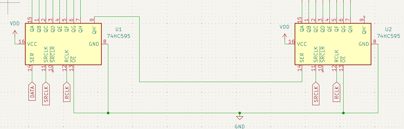
Serial Data Control for LED Drivers
In addition to controlling the matrix display logic, the CLB also autonomously generates control signals required for external shift register operation. Specifically, the CLB provides timing and synchronization signals for a 74HC595 shift register, enabling serial data transfer without CPU involvement.
Data Signal Generation
Inside the CLB, bits 8 to 11 of the CLBSWIN register are internally decoded to track the column index. A periodic DATA signal is generated and synchronized with the matrix scanning cycle.
- This DATA signal is updated once per full display refresh (i.e., every 16 columns).
- When the 4-bit column index (bits 0–3) resets to
0000 (i.e., at the beginning of a new frame), the DATA signal is briefly driven HIGH. - This rising edge can be used to shift a
1 into a chained 74HC595, effectively lighting up columns sequentially over time, creating a dynamic visual effect.
This mechanism allows the CLB to autonomously control column progression in coordination with external shift registers, without requiring manual bit manipulation from the CPU.
One-Pulse DATA Signal Generation Circuit (CLB) : A combinational CLB circuit that generates a single HIGH pulse on the DATA line every 16 cycles. It works by performing a 4-bit AND operation on the column index bits [3:0] from the CLBSWINM register. When all bits are zero (i.e., start of frame), the output of a NOT gate following the AND produces a single HIGH pulse. This signal is used to shift a new bit into the 74HC595 register chain.
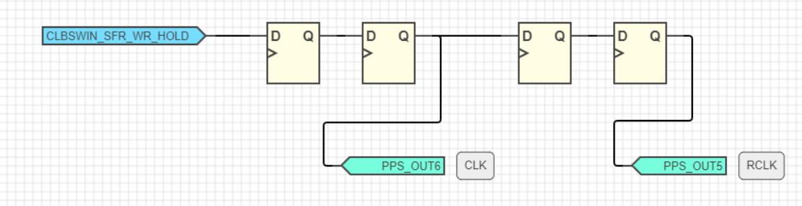
Clock Pulse Generation:
The CLBSWIN_SFR_WR_HOLD signal is internally asserted on the rising edge of the CLBSWINL write operation (i.e., whenever new 5-bit display data is written). This event triggers a short pulse after a controlled delay, implemented using two cascaded D flip-flops. The result is a clean, debounced SRCLK (shift register clock) pulse compatible with the 74HC595.
Row and Column Scanning
The CLB generates both row activation signals and column scanning logic. Columns are activated sequentially based on the column index received from the microcontroller. Only one column is active at any time, enabling multiplexed control.
Latch Pulse Generation:
A second flip-flop chain is clocked by the SRCLK signal and generates a slightly delayed RCLK (register clock or latch) pulse. This ensures that data is first shifted correctly into the 74HC595 before being latched to its output pins.
CLB-Based SRCLK and RCLK Pulse Generation Circuit : A sequential logic circuit inside the CLB that generates properly delayed SRCLK and RCLK pulses for the 74HC595 shift registers. When a write occurs to the CLBSWINL register, the CLBSWIN_SFR_WR_HOLD signal is asserted. This rising edge triggers a flip-flop to produce a short SRCLK pulse. Another flip-flop, clocked by SRCLK, creates a delayed RCLK pulse, ensuring correct timing between data shift and latch.
4. Hardware Design
4.1 LED Matrix
The LED matrix consists of 5 rows and 16 columns of LEDs arranged in a grid. Each LED can be individually controlled by selecting its row and column signals. The rows are driven directly from the microcontroller’s Configurable Logic Block (CLB), while the columns are controlled via the cascaded 74HC595 shift registers.
This arrangement allows multiplexing the display, reducing the number of required I/O pins by scanning columns one at a time and activating rows accordingly.
4.2 Shift Registers (74HC595)
LED matrix schematic showing rows and columns
Schematic showing cascaded 74HC595 connections and timing diagram
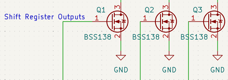
4.3 BSS138 NMOS Transistors for Current Control
The BSS138 NMOS transistors are used as current flow controllers in this design. The transistor’s drain is connected to the negative terminal of the LEDs, the source is connected to ground (GND), and the gate is driven by each output pin of the 74HC595 shift register.
When the 74HC595 output pin goes high (above the transistor’s threshold voltage), the transistor conducts, allowing current to flow from the LED cathode (drain) to ground (source), thereby turning on the LED.
This configuration provides reliable current control and protects the system by isolating the microcontroller from high current paths, ensuring stable LED operation.
BSS138 transistor schematic showing gate connected to 74HC595, drain to columns of led matrix, and source to GND
5. Software Design
The software is structured to perform real-time audio spectrum analysis with minimal CPU involvement. It is composed of three primary tasks: acquiring audio data, processing it through FFT, and transferring the result to the CLB for display. All timing-sensitive operations are handled using interrupts.
FFT Output to 16-Bar Array
Once 64 audio samples are collected via the ADC, a fixed-point Fast Fourier Transform (FFT) is executed. This transforms the audio signal from the time domain into the frequency domain. The resulting spectral data is then:
- Converted into magnitude values,
- Grouped into 16 bins (each representing approximately 1 kHz),
- Normalized and optionally filtered,
- Finally, stored in a
uint8_t array[16], where each element represents the vertical height of a single LED column (0 to 5).
This array[] is the only data structure shared with the display system, decoupling signal processing from the visualization logic.
Continuous Sampling with Timer1
Audio data is sampled continuously from the microphone using the microcontroller’s ADC. Timer1 is configured to trigger conversions at a precise rate of 32 kHz. Each ADC result is processed in an interrupt callback function, storing samples into realNumbers[]. After 64 samples, further sampling is paused until the FFT and normalization process completes. This ensures stable and non-overlapping data blocks for each FFT operation.
CLB Data Transmission via Timer2
A separate periodic interrupt, triggered every 1 ms by Timer2, handles LED matrix column updates. This interrupt does not perform any signal processing. Instead, it:
- Selects one of the 16 display columns using a static index,
- Reads the corresponding bar height from
array[], - Constructs two data bytes:
CLBSWINM: 4-bit column index + 1-bit mode information,CLBSWINL: 5-bit bar height,- Writes the values to the
CLBSWIN register pair.
This lightweight, cyclic operation ensures that the LED matrix is continuously refreshed, one column at a time, with minimal CPU overhead. Since the CLB handles the actual row/column control, the main processor is free from direct display duties.
// ADC conversion complete callback function
// This function reads the ADC value, applies DC offset correction,
// stores it in the real part array, sets the imaginary part to zero,
// and stops sampling when enough samples are collected.
void adc_callback(void)
{
    // Read the ADC conversion result
    adcVal = ADC_ConversionResultGet();

    // Apply DC offset correction and store in real part array
    // Assuming the center value of microphone signal is approximately 388
    realNumbers[indexData] = (int16_t)adcVal - 388;

    // Set imaginary part to zero for FFT input
    imaginaryNumbers[indexData++] = 0;

    // Check if required number of samples have been collected
    if (indexData >= NO_SAMPLES) {
        // Mark buffer as full and ready for processing
        bufferFull = true;

        // Reset sample index for next block
        indexData = 0;

        // Stop Timer1 to pause further sampling until processing completes
        TMR1_Stop();
    }
}
// === Sends data to CLB for one column every 1 ms ===
void my_timer2_callback(void)
{
    static uint8_t col_index = 0;

    // Read the current column's bar height (0 to 31)
    uint8_t bar_height = array[col_index];

    // Prepare lower byte: lower 5 bits represent bar height level
    uint8_t bytetosend_l = (bar_height & 0x1F);

    // Prepare upper byte: bit 4 is mode, bits 3-0 is column index
    uint8_t bytetosend_m = (mode << 4) | (col_index & 0x0F);

    // Send upper byte (mode + column index) to CLBSWINM register
    CLBSWINM = bytetosend_m;

    // **Important:** The latch signal is triggered only after writing to CLBSWINL,
    // so this register must be written last to ensure data is latched properly.
    CLBSWINL = bytetosend_l;

    // Move to the next column for the next interrupt
    col_index++;

    // Wrap around after the last column (0 to 15)
    if (col_index >= 16) col_index = 0;
}
Conclusion
The project starts with an opening animation running in animation mode. Once this animation completes, the system seamlessly switches to continuous FFT visualization mode. Due to the limited number of 5 discrete bar heights, rapid instantaneous changes in the signal are less perceptible; however, the animation mode clearly demonstrates the system’s responsiveness and speed.
The Configurable Logic Block (CLB) effectively offloads much of the processing from the microcontroller, allowing the system to operate autonomously with minimal CPU intervention. The hardware interrupts enable rapid updates, achieving a full 16 ms refresh cycle for the entire LED matrix scan, with potential for further speed improvements.
Overall, the project successfully delivers a clear spectral visualization with well-defined frequency bands, demonstrating a robust and efficient embedded signal processing and display system.