This project aims to make basic health monitoring technology (heart rate, potentially basic HRV) more accessible by implementing key processing steps on a low-cost, low-power hardware platform, suitable for affordable wearable prototypes or community health tools.
This project directly supports SDG 3: Good Health and Well-being.
The concept is :
How do we ensure 'Good Health and Well-being' when the technology itself can be a barrier?
This project confronts that challenge head-on in the world of wearable health.The core idea is to overcome the processing limitations of the PIC16F13145 MCU for real-time analysis of Photoplethysmography (PPG) signals. PPG signals, obtained by shining light (usually IR) through tissue and measuring absorption changes related to blood flow, are inherently noisy and require filtering and careful peak detection to extract heartbeats accurately.
The signal from a PPG heart rate sensor is inherently noisy; finding the true heartbeat requires constant, intensive digital filtering and nanosecond-level timing precision. For a low-cost microcontroller, this is a near-impossible software task, leading to a trade-off between accuracy, power consumption, and cost.
Our innovation is to shatter this trade-off. Instead of burdening the main processor, we offload the entire real-time signal conditioning workload to the PIC16F13145's Configurable Logic Block (CLB). We've re-imagined the CLB, treating it not as simple glue logic, but as a powerful, custom-built hardware accelerator. It filters the noise and pinpoints the heartbeat in hardware, then simply tells the main processor when a beat occurred.
This dramatically changes the game.
The MCU is free to handle user interface, data transmission, and more complex analysis like HRV. It's a paradigm shift that enables high-fidelity performance on a low-cost platform, directly paving the way for accessible health monitoring tools that can make a real-world impact. This project offloads the critical, real-time pre-processing steps like filtering, peak detection, and precise timing to the CLB, treating it as a dedicated hardware co-processor.
CLB Implementation Details
Input Signal Path:
- An analog PPG signal, acquired from a sensor, is first amplified.
- This amplified signal is then fed into an ADC channel on the PIC16F13145, where it is digitized to an 8-bit result to optimize resource usage.
Advanced Use:
- The CLB can still be programmed to generate precise timing pulses for the PPG sensor's LED and to trigger the ADC sampling in perfect synchronization. This technique is highly effective for ambient light rejection and remains a key demonstration of the CLB's capabilities for system-level control.
- The 8-bit digitized result from the ADC is routed internally to the CLB input for real-time processing.
CLB Processing Pipeline & MCU Peripheral Integration:
The processing is split between the CLB (for custom logic) and the MCU's hardware timers (for standard timing).
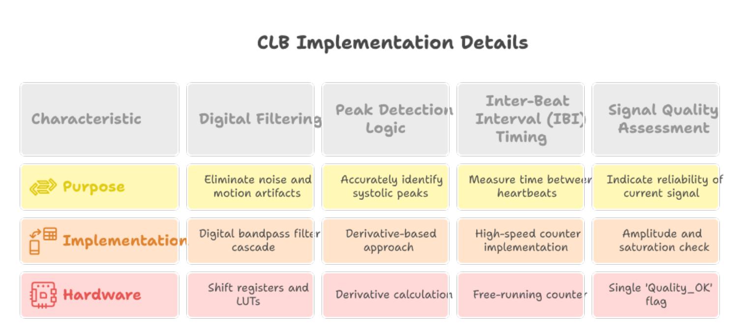
(Block 1) Digital Filtering (in CLB):
- Purpose: To eliminate DC offset and high-frequency noise, isolating the ~0.5-3Hz heartbeat signal.
- Implementation: To fit within the CLB's tight resource limits, a highly efficient first-order IIR (Infinite Impulse Response) low-pass filter is used.
- The equation y[n] = (1/8)*x[n] + (7/8)*y[n-1] is implemented, where the multiplications are replaced by simple, fast bit-shift operations.
- Hardware: This efficient design requires only a single 8-bit register (DFFs) to store the previous output and combinational logic (LUTs) for the required add/subtract/shift operations.
(Block 2) Peak Detection Logic (in CLB):
- Purpose: To accurately identify the systolic peaks within the filtered PPG waveform.
- Implementation: A derivative-based approach is used on the 8-bit filtered signal. A peak is identified when the signal's slope (calculated as filtered[n] - filtered[n-1]) changes from positive to negative.
- Output: The CLB's final output is a single, clean clock-cycle pulse ( for each detected heartbeat. This is the sole output from the CLB pipeline.
(Block 3) Inter-Beat Interval (IBI) Timing (CLB + MCU Peripherals):
- Purpose: To measure the precise time elapsed between consecutive heartbeat pulses.
- Implementation: This critical task is offloaded from the CLB to the MCU's dedicated hardware peripherals for maximum precision and efficiency.
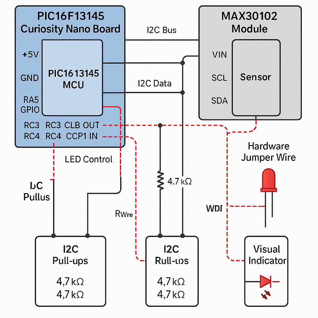
- The Peak_Detected_Pulse from the CLB is routed from a CLB output pin to a CCP (Capture/Compare/PWM) input pin on the MCU.
- The MCU's TMR1 peripheral is configured as a fast, 16-bit, free-running hardware counter.
- The CCP module is set to Capture Mode. When it detects the rising edge of the pulse from the CLB, it automatically and instantly copies the current value of TMR1 into its hardware register (CCPR1) and triggers an MCU interrupt.
- This hybrid approach uses the CLB for what it does best (custom real-time logic) and the MCU's peripherals for what they do best (standardized, precise timing), saving immense CLB resources.
Advanced CLB Use :
- Hardware Co-processing: The CLB is used as a custom-tailored, real-time DSP front-end for bio-signal filtering and feature extraction.
- Real-time Pipelined Architecture: The CLB implements a filter-then-detect pipeline that processes ADC data with zero MCU intervention.
- Timing Criticality: The CLB provides the critical, real-time heartbeat trigger, while precise timestamping is offloaded to the MCU's dedicated CCP/Timer peripherals, demonstrating a powerful and efficient hybrid hardware architecture.
- System Synchronization: The CLB can be used for advanced tasks like synchronizing the sensor's LED pulses with ADC sampling to improve signal-to-noise ratio.
MCU Role
The PIC16F13145's main core will be responsible for the higher-level logic.
- Configuration: Initialize and configure the CLB with the designed logic, set up the ADC, and control the PPG sensor's parameters.
- Data Acquisition & Processing: On an interrupt from the CLB, the MCU will read the latched timestamp and the signal quality flag. It will then calculate the IBI by subtracting the current timestamp from the previous one and compute the Heart Rate (HR = 60 / IBI in seconds). Basic HRV metrics like SDNN can also be calculated from a buffer of recent IBIs.
- Application & Interface: The MCU will display the calculated heart rate, for instance, via UART to a computer terminal or on a small LCD. It can also provide visual feedback, such as blinking an LED in time with the detected heartbeat.
Design:
Creating a full, compilable project of this complexity involves several distinct stages, especially since a significant portion of the logic resides within the Configurable Logic Block (CLB), which is designed with a Hardware Description Language (HDL).
1)Implement a first-order IIR low-pass filter: y[n] = (1/8) * x[n] + (7/8) * y[n-1]. The divisions by 8 are implemented as simple 3-bit right shifts, making it extremely efficient. - iir_filter_8bit.v , Resources: ~8 DFFs, ~10 LUTs.
2)Take the filtered signal and identifies the peaks using a derivative-based approach but operating on an 8-bit data path. - peak_detector_8bit.v, Resources: ~18 DFFs, ~10 LUTs.
1)Implement a first-order IIR low-pass filter: y[n] = (1/8) * x[n] + (7/8) * y[n-1]. The divisions by 8 are implemented as simple 3-bit right shifts, making it extremely efficient. - iir_filter_8bit.v
2)Take the filtered signal and identifies the peaks using a derivative-based approach but operating on an 8-bit data path. - peak_detector_8bit.v
MCU Configuration
by using MPLAB X IDE and the MCC plugin:
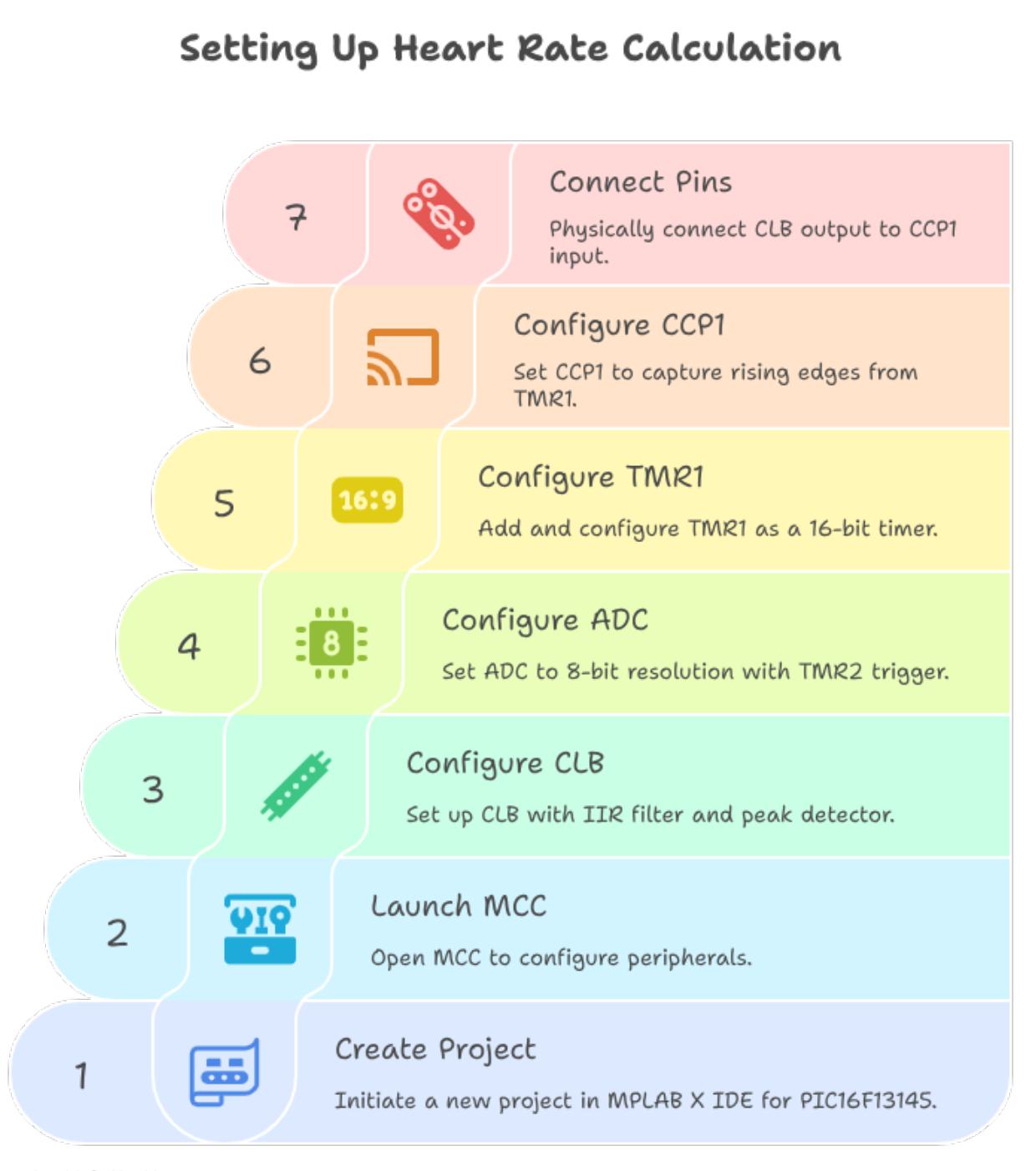
- Create a New Project: In MPLAB X IDE, create a new standalone project for the PIC16F13145.
- Launch MCC: Open MCC.
- CLB:
- In the CLB Synthesizer, use the new iir_filter_8bit.v and peak_detector_8bit.v files.
- Connect them: ADC_OUT -> IIR_IN, IIR_OUT -> PEAK_DET_IN.
- The only output from the CLB that you need to route to a pin is the peak_detected_pulse. Assign it to the pin that corresponds to the CCP1 input.
ADCC (ADC):
- In the ADC configuration, set the Result Size to 8-bit.
- Keep the ADC trigger source (TMR2) to maintain a consistent sampling rate.
TMR1 :
- Add the TMR1 peripheral to your project.
- Configure it as a 16-bit Timer.
- Set its clock source (FOSC). This frequency is needed for the final heart rate calculation.
- Let it be a free-running counter.
CCP1 :
- Add the CCP1 peripheral.
- Set its mode to Capture.
- Set the Capture Trigger to "Every rising edge".
- Set the Capture Timer Source to TMR1. This links the CCP module to your timer.
- Enable the CCP interrupt.
Pin Manager:
- This is the most important step. You must create an external connection with a wire.
- Find the physical pin you assigned as the CLB output (peak_detected_pulse).
- Find the physical pin assigned as the CCP1 input.
- Connect these two pins on your development board with a physical jumper wire.
- The signal cannot be routed internally on this device.
BOM:
To make this project as accessible as possible, we've provided two distinct Bills of Materials.
The first path uses a pre-built sensor module, which is the fastest way to get started and allows you to focus entirely on the core innovation: our CLB co-processor.
The second, more advanced path, shows how to build the entire sensor circuit from scratch using discrete components, demonstrating a deeper level of analog hardware design and utilizing the bonus Microchip op-amp.
Schematic (Sensor implementation)
Schematic (Discreet parts implementation)