This laser tag system module uses the PIC16F13145’s Configurable Logic Block to handle 38kHz signal transmission and decoding, offloading timing-critical tasks from the CPU. This proof-of-concept uses the onboard switch for firing and LED for hit indication enabling efficient real-time gameplay with room for expansion via a UART API.
1. Introduction
1.1 Project Overview
This project aims at developing a Configurable Logic Block (CLB) based module for encoding and decoding IR signals using the Sony Infrared Remote Control (SIRC) protocol. Developing such a module would be the basis for an open-source laser tag system with standardized, interoperable communication.
1.2 Motivation
The development of a custom laser tag system utilizing a CLB-based SIRC encoder/decoder module is driven by the desire to create a more efficient, modular, and scalable solution for the system’s necessary infrared communication. Previous implementations of the SIRC protocol on microcontrollers have often heavily relied on a combination of several hardware modules and software-based encoding and decoding. This heavy reliance on the microcontroller’s resources can burden the CPU and complicate system development. This project aims to address these limitations by attempting the following:
Hardware Offloading via CLB
By implementing the SIRC protocol in the CLB hardware of the microcontroller, time-critical encoding and decoding tasks can be offloaded from other peripheral hardware modules and the CPU core.
Reduced Software Overhead
Offloading the SIRC protocol to the CLB significantly reduces the computational load on the microcontroller. This frees up processor cycles for higher-level game logic and peripheral interaction which leads to an improved overall system responsiveness.
Standardized Modular Communication Layer
The CLB-based module acts as a self-contained communication subsystem. A modular design would simplify its integration, testing, and reuse across multiple projects or device platforms, while also promoting a level of standardization in protocol implementation for future open-source initiatives.
Improved Compatibility with Resource-Limited Devices
Some popular embedded platforms lack the timing accuracy or hardware resources needed to reliably implement SIRC encoding/decoding. The CLB module abstracts away these requirements which would allow seamless integration even with devices that would otherwise be incapable of handling this load.
2. Methodology and System Design
2.1 Overview of SIRC Protocol
The Sony Infrared Remote Control protocol is a communication standard previously used by Sony remote controls to transmit data to electronic devices via infrared (IR) signals. It operates using a modulated carrier frequency and transmits data in messages composed of a 2400 μs header pulse followed by a series of data bits. Each bit is represented by a pulse followed by a space: a logic '1' has a 1200 μs pulse while a logic '0' has a shorter 600 μs pulse. The protocol is known for its simplicity and reliability which explains why other laser tag projects, such as the MilesTag 2 protocol, utilizes the SIRC protocol with a 38kHz carrier frequency. It should be noted that IR Decoder components are commercially available to demodulate the modulated carrier signal. The resulting decoder signal is an active low output.
Figure 1 - SIRC Protocol Timing Diagram
2.2 SIRC Module Design
For this project, the SIRC module design will be divided into two primary functional blocks to handle infrared communication: SIRC TX for signal encoding and transmission, and SIRC RX for signal reception and decoding. This separation of responsibilities ensures clear modularity, allowing each block to be designed and tested independently. The following subsections provide further details on both TX and RX functional blocks.
2.2.1 SIRC TX
The composition of the SIRC header, logical ‘0’ and logical ‘1’ bits can be simplified down to a series of 600 μs pulses. As can been seen in Figure 2, a header requires four high pulses followed by a single low pulse. A logical ‘1’ requires two consecutive high pulses followed by a low pulse while a logical ‘0’ only requires a single high pulse followed by a low pulse. As a result, a message comprised of data bits can be transformed into a pulse stream which specifies when the carrier frequency must be turned on or off.
Figure 2 - SIRC TX Signal Generation Diagram
The use of the laser enable variable, as a third input to the SIRC TX module, is desirable as it allows the system to quickly check the transmission status of the laser without having to know the current message’s pulse stream index and its overall length. The output signal therefore only requires a 3 input AND gate to generate the desired SIRC signal.
The pulse width modulation hardware, PWM1, was used to create the 38kHz carrier signal source. On the PIC16F13145, the PWM hardware can only select Timer 2 to enable its functionality and was therefore used as well. A second timer, Timer 1, was used to generate an interrupt every 600 μs to update the pulse stream index along the message’s pulse array values. As can be seen in Figure 3, the CLB module took the PWM1 output signal, and both the Laser Enable and Carrier Enable software values as inputs to a 3 input AND gate to create the desired SIRC TX output (i.e. the laser signal).
Figure 3 - SIRC TX CLB Implementation
The design aimed at having two possible sources to trigger the start of a signal transmission: An external interrupt tied to a I/O pin and the UART module. A diagram of the overall microcontroller’s hardware configuration can be found in Figure 4 while flowcharts of the ISRs can be found in Figure 5.
Figure 4 – PIC16F13145 Hardware Configuration for SIRC TX Functional Block
Figure 5 – ISRs Flowcharts for SIRC TX Functional Block
2.2.2 SIRC RX
Several options exist to decode an incoming SIRC signal. Many of these options are aimed at measuring the duration of pulses to determine if a logical ‘0’ or ‘1’ was transmitted. These approaches could be implemented using timers and Capture/Compare/PWM (CCP) hardware modules. Unfortunately, after the implementation of the SIRC TX block, the PIC16F13145 only has one timer remaining (Timer 0). Furthermore, since this microcontroller’s CCP modules require the configuration and use of Timer 2 for their functionality, these modules are also not available for the SIRC RX block. The design therefore needed to have the SIRC RX block offload as much of its hardware needs to the CLB such that it did not need to rely on too many additional hardware modules that were still available.
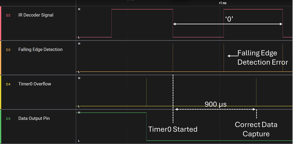
Upon further observation, it is possible to determine the value of the data bit based on the state of the incoming signal 900 μs after the falling edge occurs of the start the first pulse of each new data bit. As can be seen in Figure 6, the value of the incoming signal at that point is the inverse of the actual data bit value.
Figure 6 – IR Decoder Signal Data Capture Timing Diagram
At first glance, it would seem logical to set the period of Timer 0 to 900 μs such that the signal value could be measured after the timer was triggered to start with the falling edge of the signal. However, since the implementation of a header detection solution is also still required for the SIRC RX block, attempts should be made to utilize Timer 0 for both header detection and data interpretation since both pulses cannot occur at the same time. Given that the header pulse is 2400 μs and data pulse capture length is 900 μs, the highest common factor is 300 μs. If the Timer 0 period is set to 300 μs, a 3-bit counter will be needed to detect the 2400 μs header pulse (300 μs * 23 = 2400 μs).
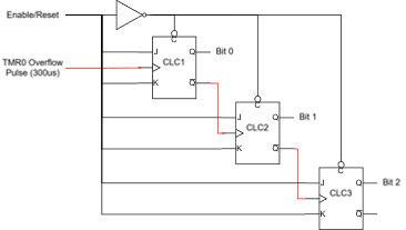
Keeping in mind our stated objective of reducing software overhead, it would be ideal to design this counter in hardware rather than relying solely on an interrupt software solution. Based on the remaining hardware modules available, an asynchronous counter using 3 CLC modules configured as J-K flip-flops was designed (see Figure 7). Along with the Timer 0 overflow pulse used as a clock input, the counter also includes an enable/reset line to both clear and disable the counter.
Figure 7 – CLC-base 3 Bit Asynchronous Counter Implementation
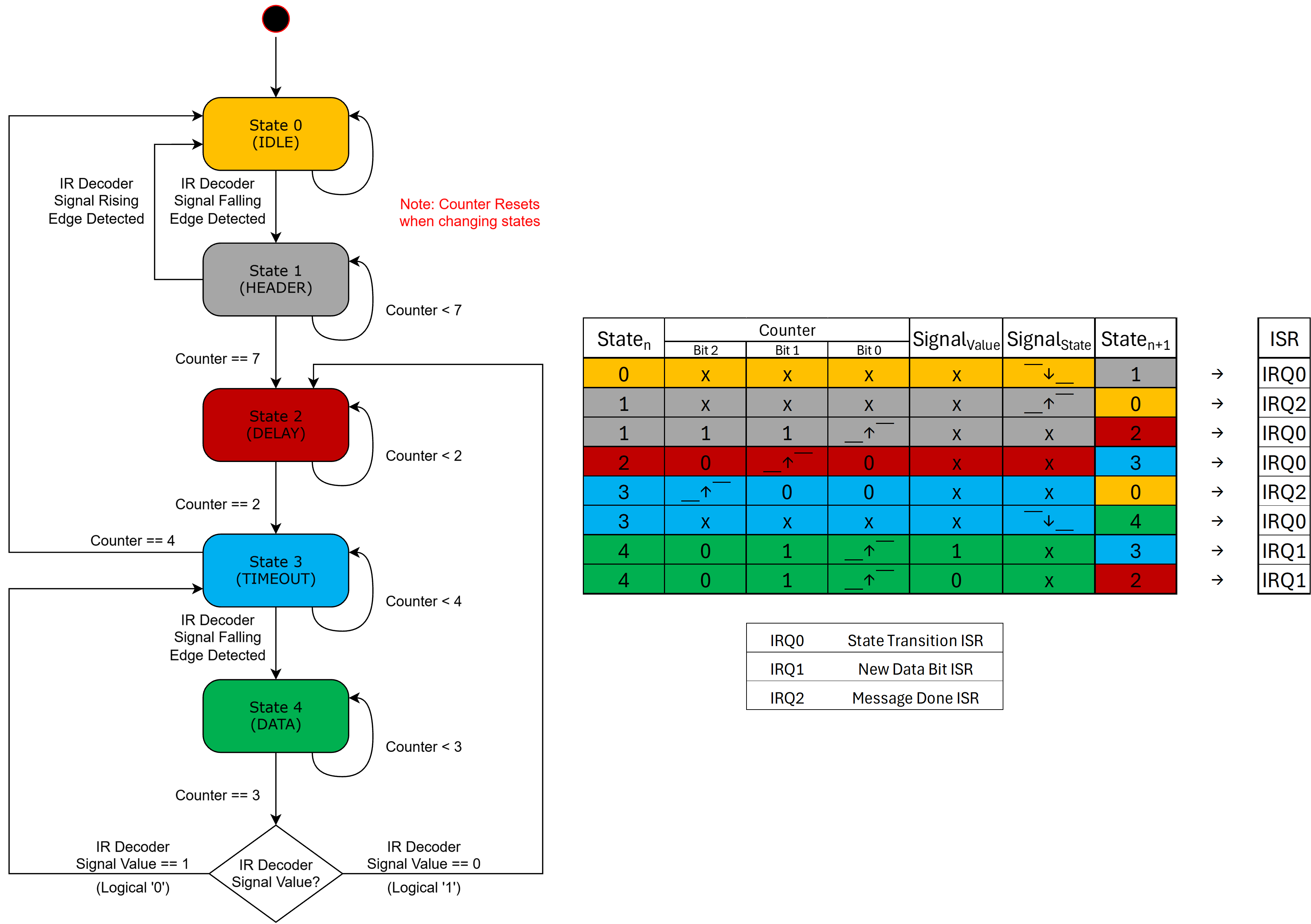
Having a hardware counter and edge detection capabilities, a finite state machine (FSM) was developed for the following states:
State 0 (Idle)
No activity has been detected, and the input signal is in the inactive state (i.e. High).
State 1 (Header)
Falling edge has been detected, waiting to see if this is a header pulse with no early rising edge occurrence.
State 2 (Delay)
Delayed period to allow rising edge to occur prior to moving to the following state.
State 3 (Timeout)
Waiting for either a falling edge to occur or for the counter to ‘timeout’ to indicate the end of the message.
State 4 (Data)
Falling edge has been detected. Waiting 900 μs before determining the new data bit value.
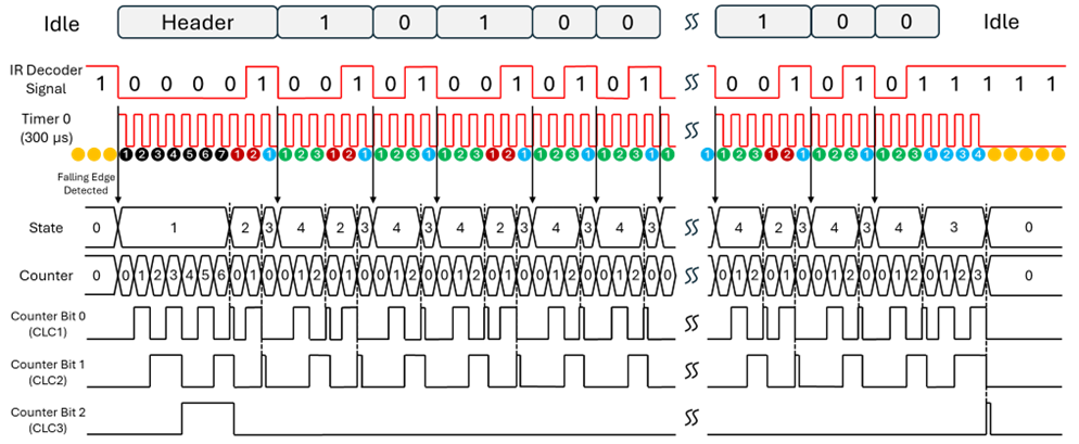
With the timer 0 period and the states for the FSM defined, an evaluation of a SIRC signal along with the development of a flowchart of the FSM attempted can be seen in Figures 8 and 9, respectively.
Figure 8 – SIRC RX Timing Diagram
Figure 9 – SIRC RX FSM Flowchart and Table
With the FSM flowchart and transitions established, its implementation could be attempted in the CLB block. The overall SIRC RX functional block, along with the CLB implementation, can be found in Figures 10 and 11, respectively. Flowcharts of the CLB ISRs can be found in Figure 12.
Figure 9 – SIRC RX FSM Flowchart and Table
Figure 11 – SIRC RX CLB Implementation
Figure 12 – ISRs Flowcharts for SIRC RX Functional Block
3. Hardware Implementation and Results
Having all the functional blocks designed and their associated hardware modules configured, the next step was to compile and program the PIC16F13145 Curiosity Nano board and to connect some external circuitry to allow for both the transmission and reception of SIRC signals. To simplify the signal transmission and improve its range, the circuitry used was based on using a red laser module, an IR decoder module, a few transistors, some photodiodes, and an IR LED. The final hardware configuration can be found in Figure 13. Interacting with the system could be done by using the onboard switch (SW0) or using the microcontroller’s UART. To simplify the UART communication, an API format was created as a template for future configuration capabilities (see Appendix A).
Figure 13 – PIC16F13145 Hardware Circuit Setup
3.1 Signal Transmission Testing
The first test focused on evaluating the SIRC TX module’s ability to transmit the proper signal when pressing the PIC16 Curiosity Nano’s onboard button to shoot the laser. The signal was validated by connecting a Saleae Logic Analyzer to the SIRC TX output pin and can be seen in Figure 14.
Figure 14 – Logic Analyzer Capture of Generated SIRC TX Signal
3.2 Signal Decoding Testing
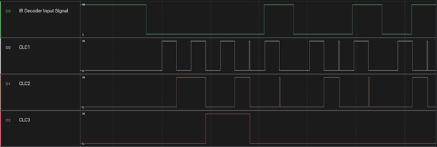
The next test focused on verifying the proper function of the CLB-based SIRC RX module. For this test, a Sony RM-LP204 remote was used to generate different SIRC signals. The logic analyzer was connected to several pins to measure both the incoming signal and the CLC-based counter output (which were connected to the pins using the PIC16’s Peripheral Pin Select module). The received messages were also sent to the UART module which was connected to a RealTerm Software Terminal. Confirmation of the SIRC RX module can be seen in Figures 15 and 16.
Figure 15 – Logic Analyzer Capture of CLC Output for CLB FSM Validation
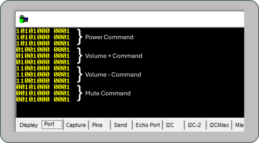
Figure 16 – RealTerm Capture (with Annotation) of SIRC RX Decoded Output Sent Over UART
3.3 Full System Interaction
The final test consisted of using the UART API to send a "Shoot Laser" command to fire the laser. Any received message from the SIRC RX module would be sent out to the UART. In order to properly perform this test, two PIC16F13145 Curiosity Nano boards were used. One board was configured as Player 3 from Team 2 while the second board was configured as Player 12 from Team 3. The shot damage for both devices was set to 100, The successful operation of the entire system can be seen in Figure 17. In this test, the boards took turns to send one shot command.
Figure 17 – Logic Analyzer Capture of TX/RX Transmission Between Laser Tag System on Two PIC16 Curiosity Nano Boards
4. Discussion
The development of a CLB-based SIRC module resulted in a functional and robust solution even in light of some obstacles that were encountered along the way. These challenges, along with how they were addressed, are described in further detail below.
4.1. Flickering on IR Decoder Signal During Rising Edges
The initial design for the SIRC RX module tried to mimic a similar approach used by the CLB based Manchester Decoder example on the MPLAB Discover webpage by using a 900 μs timer period as seen in Figure 18.
Figure 18 – Initial SIRC RX CLB Concept Design
It was discovered, during initial testing of this design, that the IR Encoder input signal sometimes had some flicker during transitions (Figure 19).
Figure 19 – IR Encoder Input Signal ‘Flicker’ Behaviour
These false falling edges did not have any effect during the transmission of a logical ‘0’ given that Timer 0 was already running (Figure 20).
Figure 20 – False Edge Detection During Logical ‘0’
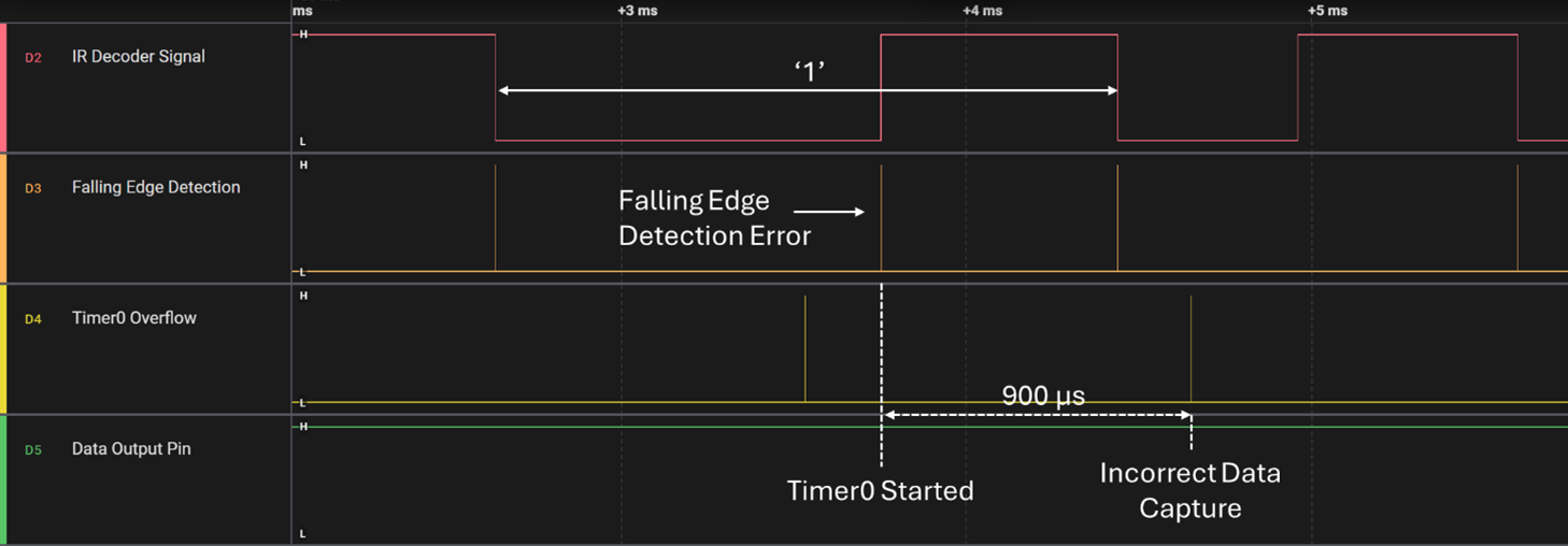
They did however have an effect during a logical ‘1’ transmission given that it would restart Timer 0 before the falling edge of the next data bit (Figure 21).
Figure 21 – False Edge Detection During Logical ‘1’
Given that we cannot guarantee that the incoming IR decoded signal is free of this jitter noise, it would be prudent to try and avoid using any edge detection during the time window where a rising edge on the input signal is expected to occur. This IR decoder behavior resulted in the redesign of the SIRC RX module into a state machine which included a ‘Delay’ state to wait a fix period of time (600 μs) during which the rising edge of the signal should have occurred before moving to the next state.
4.2 Routing Internal Signal to CLC Input
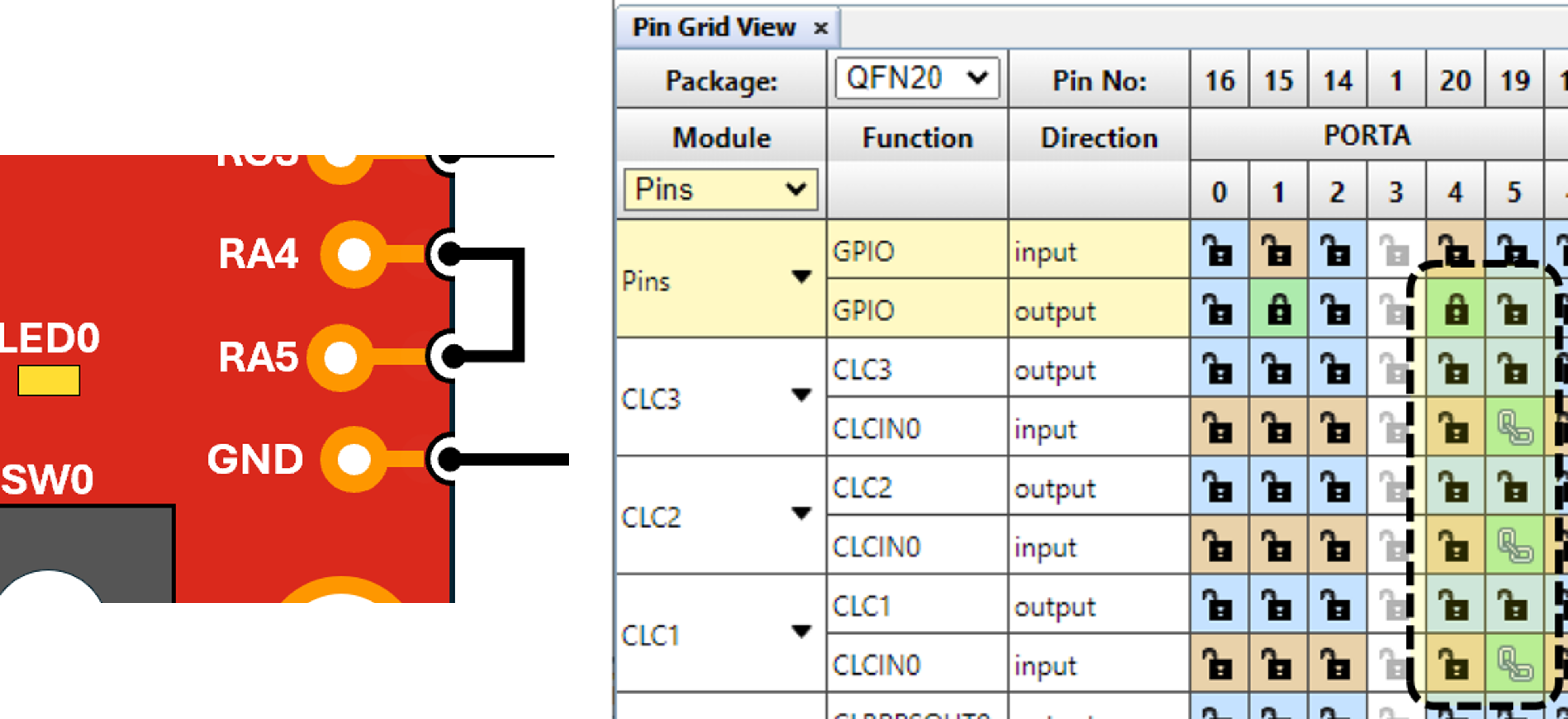
The SIRC RX block required the use of a CLC-based counter which used the Timer 0 overflow pulse as its clock and an additional signal to enable/reset the counter. Unfortunately, this signal is not one of the configurable input sources available in the CLCnSLE0 register. In order to solve this problem, CLCIN0PPS was selected as the input source and tied to pin 5 of Port A while the pin 4 of Port A was configured as an output pin for the enable/reset value. This required a physical jumper between the two pins on the PIC16F13145 Curiosity Nano board.
Figure 22 – Enable/Reset Pin Jumper Solution for CLC Input
5. Conclusion
The development and implementation of the CLB-based SIRC encoder/decoder proved to be a successful and effective solution for the laser tag project. The system demonstrated robust and consistent performance, achieving reliable signal encoding and decoding using the available hardware resources. By leveraging the capabilities of the CLB, the design remained compact without overburdening the CPU. Furthermore, the modular nature of the system, along with the use of a simple UART-based API, allows it to be easily adapted as a SIRC interface for other embedded system projects. This provides huge potential to allow the design to not only be efficient but also highly reusable and scalable for a wide range of other open-source applications based on the SIRC protocol.
5.1 Future Work
This project utilized the PIC16F13145 Curiosity Nano board connected to only a few components to provide a proof-of-concept system for the CLB-based design. To further advance the laser tag system, user configuration could be improved with the addition of physical controls (switches/LEDs) and/or the use of the ADC hardware (with potentiometers) for team/player setup. The expansion/implementation of additional UART API functions would also facilitate the configuration of enhanced control and gameplay features.
Additionally, the project would benefit from the design of a proper casing for the laser tag module. The design would include a proper trigger switch, visual display for user feedback, and incorporate the sensor module. Audio feedback could also be integrated with the use of a voice playback module. These off-the-shelf devices can often be controlled via a simple UART interface. Although the PIC16F13145 only has one UART module, both the laser tag API and voice playback module could be supported through the use of the microcontroller’s Peripheral Pin Select (PPS) module to alternate the UART connections between two different pairs of RX/TX pins.
Finally, to allow others the flexibility to use this CLB-based SIRC module for laser tag (or any other project), a mikroBus add-on board could be developed. It would include the PIC16F13145 microcontroller along with the necessary components to connect both the laser and sensor modules. Communication with the board would be done through the UART pins defined by the mikroBus standard.
6. References