This project demonstrates the PIC16F13145 Curiosity Nano's Configurable Logic Block (CLB) capabilities through a real-time monitoring system. The design uses the CLB to offload threshold analysis from the MCU. Hardware-accelerated processing achieves fast response for vital sign monitoring while consuming only 84% of available CLB resources.
Introduction
Real-time health monitoring demands both precision and efficiency – a challenge for conventional MCU designs. This project solves it using the PIC16F13145 Curiosity Nano’s Configurable Logic Block (CLB) to hardware-accelerate vital sign analysis. By offloading temperature and pulse threshold checks to the CLB, the system achieves deterministic response times while reducing MCU workload. The design creatively repurposes the CLB for dual signal processing: a temperature monitor (20-25°C range) and a BPM monitor (60-100 BPM), demonstrating advanced peripheral integration. MPLAB Code Configurator simplified setup, proving the solution’s accessibility. Developed for the 2025 Configurable Logic Design challenge, this work showcases how programmable logic can enhance embedded medical devices. Complete documentation is available for evaluation and practical guide for implementation.
What it does?
This system monitors two vital parameters in real-time: ambient temperature and cardiac activity. The LM35 temperature sensor's analog readings are digitized by the ADC, processed through CLB logic to determine thermal ranges (20-25°C), and displayed via UART alongside status LEDs. Simultaneously, an IR reflectance circuit detects pulse signals, with the CLB validating each beat through hardware-level threshold analysis. Finally, Timer-driven BPM calculations (60-100 BPM range) are evaluated by the CLB, triggering visual alerts when values exceed clinically safe thresholds. All processing occurs by using hardware logic on the CLB.
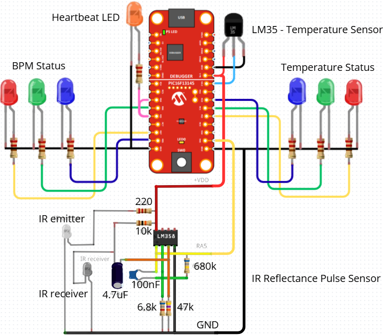
General Schematic Overview
Why it's cool?
The real magic lies in how the Configurable Logic Block transforms ordinary sensor monitoring. By implementing temperature checks, pulse validation, and BPM analysis in programmable logic, the system achieves three unique advantages:
- Zero-latency threshold detection (vs. software delays)
- Parallel processing of multiple signals in one hardware block
- Component efficiency versus MCU-only solutions
This isn't just sensor monitoring - it's hardware-accelerated health tracking that leaves 16% of CLB resources available for future upgrades like SPO₂ integration. The Curiosity Nano makes this advanced functionality accessible through MPLAB's intuitive tools, proving complex embedded design can be both powerful and approachable.
CLB Logic Implementation
The Configurable Logic Block serves as the system's hardware accelerator, handling three critical tasks in parallel: Thermal Range Evaluation; Pulse Validation; Cardiac Rhythm Analysis.
Each function operates independently through Verilog components while sharing LUT resources efficiently (84% utilization). This hardware-based approach eliminates the timing variability inherent in software solutions.
Temperature Logic
The system establishes temperature ranges through precise ADC value mapping. Using the LM35's linear 10mV/°C output scaled to the 10-bit ADC (3.3V reference), thresholds are set at:
- Lower Limit: 20.32°C → 63 (00111111₂)
- Upper Limit: 24.84°C → 77 (01001101₂)
Full calculations are described on the Complete documentation.
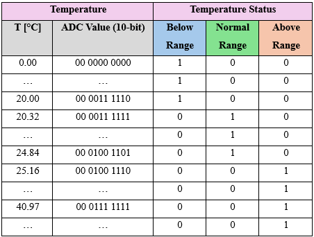
These values optimize CLB resource usage while maintaining ±0.5°C resolution. The decision logic follows this truth table:
Temperature State Truth Table
Analysis of the encoding scheme reveals that only the 7 least significant bits (bits 0-6) of the ADC value are required to monitor temperatures up to 40.97°C. This efficient bit allocation allows the CLB to process thermal data while conserving logic resources. For applications requiring extended range detection up to 82.26°C, the system can optionally incorporate bit 7 into the evaluation logic. The implementation employs a Verilog module that continuously analyzes these 7 bits to classify the current temperature state, demonstrating how programmable logic enables adaptable threshold detection without MCU intervention.
module comp (bit0, bit1, bit2, bit3, bit4, bit5, bit6, LOW, NORMAL, HIGH);
    input bit0, bit1, bit2, bit3, bit4, bit5, bit6;
    output LOW, NORMAL, HIGH;
    assign LOW = !bit6 & (~(bit5 & bit4 & bit3 & bit2 & bit1 & bit0));
    assign HIGH = bit6 & (bit5 | bit4 | (bit3 & bit2 & bit1));
    assign NORMAL = !(LOW|HIGH);
endmodule
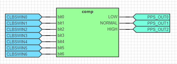
By integrating this component into the main design and configuring its software inputs and hardware outputs, the resulting implementation yields:
Resulting CLB component with I/O mapping
The Verilog component was functionally validated using the CLB Synthesizer's Test bench prior to implementation, confirming correct state classification across all temperature ranges. Physical outputs were assigned through MPLAB's pin grid view, with thermal status indicators routed to: RC0 (LOW), RC1 (NORMAL), and RC2 (HIGH) for LED visual feedback.
Beat Detection Logic
The CLB's second critical function processes pulse signals from the IR reflectance sensor, digitized through the MCU's ADC channel (ANA5). Initial characterization with MPLAB Data Visualizer established clear detection thresholds: a valid pulse registers at 598 (10 0101 0110₂), while baseline noise measures 0 (00 0000 0000₂). To optimize performance, the system leverages ADC bit 9 (512 or 10 0000 0000₂) as the detection threshold, reducing the comparison to a single-bit operation. This hardware-based approach eliminates software processing overhead entirely.
The implemented design masks and right-shifts the pulse sensor's ADC bit 9 to bit 7 position, enabling efficient data packing with the 7-bit temperature values for transmission via CLBSWIN7. This word structure optimization, detailed in the BPM Logic section, demonstrates how the CLB enables compact, hardware-accelerated signal processing.
Resulting CLB logic for Beat Detection with I/O mapping
BPM Logic
The system utilizes Timer1 as a precision pulse counter, accumulating beats during fixed 10-second windows determined by Timer0 overflows. This hardware-timed approach enables accurate BPM calculation in firmware while maintaining deterministic sampling intervals. Although a pure CLB-based frequency counter would offer marginal performance gains, the current hybrid solution (MCU counting + CLB thresholding) provides optimal development efficiency for this implementation.
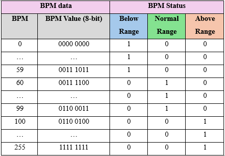
The CLB's third critical function evaluates calculated BPM values against clinical thresholds (60-100 BPM), with out-of-range conditions triggering visual alerts via LEDs or optional buzzer/notification systems. This range aligns with American Heart Association guidelines, where values below 60 BPM indicate bradycardia and readings above 100 BPM suggest tachycardia. The logic encodes these thresholds as binary values: 60 BPM (00 0011 1100₂) and 100 BPM (00 0110 0100₂).
A dedicated Verilog module processes the 8-bit BPM value (packed into the CLBSWIN register's upper byte) to determine cardiac status. The truth table formalizes the state classification logic, demonstrating how the CLB simultaneously handles both temperature and cardiac rhythm analysis within its 84% utilized resources. This dual-function implementation showcases the Curiosity Nano's capacity for mixed-signal health monitoring applications.
CLB BPM State Truth Table
To optimize CLB throughput, the system employs an efficient 16-bit word structure. The BPM value is masked and left-shifted to occupy bits 15-8, while the 7-bit temperature data occupies bits 6-0, with pulse detection status at bit 7. This packed format transmits via the CLBSWIN register, minimizing bus transactions. The firmware implementation handles this data packing during each sampling interval.
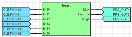
The Verilog component designed to satisfy the above table is described as:
module heart(bit10, bit11, bit12, bit13, bit14, bit15, hlow, hnormal, hhigh);
    input bit10, bit11, bit12, bit13, bit14, bit15;
    output hlow, hnormal, hhigh;
    assign hlow = !(bit15 | bit14) & !(bit13 & bit12 & bit11 & bit10);
    assign hhigh = bit15 | (bit14 & bit13 & (bit12 | bit11 | bit10));
    assign hnormal = !(hlow | hhigh);
endmodule
By integrating this component into the main design and configuring its software inputs and hardware outputs, the resulting implementation yields:
Resulting CLB component with I/O mapping
Firmware Configuration
CLB Configuration via MCC
The development process begins by adding the CLB peripheral through MPLAB Code Configurator's Application Builder interface. This action automatically launches the integrated CLB Synthesizer tool, where the three core logic components (temperature threshold detector, pulse validator, and BPM analyzer) are implemented in the main sheet. The synthesizer provides real-time feedback on resource utilization and enables functional simulation to validate logic behavior before hardware deployment.
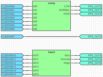
Thus, the CLB sheet ends looking like this:
CLB Synthesizer Implementation
Peripherals Configuration
The ADC setup begins by adding its API through MCC, where ANA2 is designated as the primary positive input channel for temperature sensing. While the system ultimately utilizes two ADC channels (ANA2 for temperature and ANA5 for pulse detection), MCC requires to initialize at least one of the channels used, with remaining channel assignments completed later in the Pin Management Section.
UART configuration maintains the default 9600 baud rate while enabling the critical printf redirection feature. This functionality proves invaluable for real-time system monitoring and debugging, allowing serial output of sensor readings and status alerts without additional coding overhead.
For timing operations, Timer0 is configured with the LFINTOSC (31 kHz) clock source, precisely tuned to generate 10-second overflow intervals - the foundation for accurate BPM calculation. This hardware-timed approach ensures consistent sampling periods independent of firmware execution flow. Meanwhile, Timer1 operates in counter mode, incrementing with each validated pulse detected through the T1CKIPPS external clock input.
While this overview highlights the key aspects of each peripheral setup, complete implementation details are documented in the Complete documentation for reference.
Pin Management
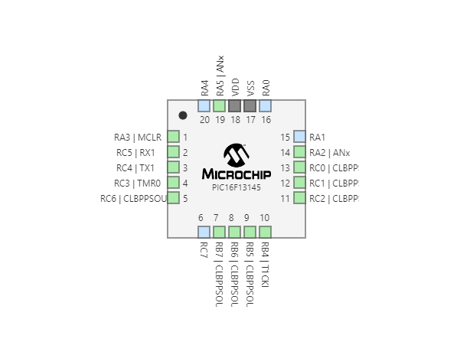
The system's physical I/O configuration was finalized through MCC's Pin Grid View, which provides visual verification of signal routing and peripheral conflicts. Key assignments include analog inputs (ANA2 for LM35, ANA5 for pulse detection), timer clock sources (T1CKIPPS on RB4), and CLB-driven outputs (RC0-2 for temperature status, RC6 for pulse verification and RB5-7 for BPM status). It also uses RC3 as TMR0 output to visualize the sampling time. This centralized interface ensures proper voltage level matching and avoids resource collisions when using different peripherals.
Firmware Implementation
With all peripherals configured through MCC, the system generates optimized initialization code via Project Resources > Generate. This automation produces production-ready boilerplate while preserving custom logic integration points. The main application code implements the real-time monitoring workflow as follows:
#include <xc.h>
#include "mcc_generated_files/system/system.h"

#define LM35_SCALE_FACTOR    3.3*100/1023  // ADC → °C (Using VDD as Positive Voltage Reference)
#define HEART_RATE_BIT_MASK  0x0200              // Bit 9 of Heart_Value
#define TEMP_BIT_MASK        0x007F              // Bits 0-6 of LM35_Value
// Heart Rate
uint8_t BPM;                // Beats per minute
uint32_t Heartbeat_Count;   // Total beats in 10-second window
int16_t Heart_Value;        // Raw ADC value from heartbeat sensor
// Temperature
int16_t LM35_Value; // Raw ADC value from temperature sensor
float Temperature;  // Room temperature
// CLB
int16_t CLB_data; // Data sent to the CLB
// Timer0 toggles each 10 seconds
void Timer0Callback(void)
{
    BPM = (uint8_t) Heartbeat_Count * 6; // BPM = (Beats counted in 10 seconds) * 6
    TMR1_CounterSet(0);                  // Resets the Heartbeat_Count
}
int main(void)
{
    // Initialize the peripherals and enables the interrupts
    SYSTEM_Initialize();
    INTERRUPT_GlobalInterruptEnable();
    INTERRUPT_PeripheralInterruptEnable();
    printf("Starting the device...\r\n");   // Sends a message to the terminal
    TMR0_OverflowCallbackRegister(Timer0Callback); // Enables Timer0Callback
    TMR1_CounterSet(0);                // Initializes the Heartbeat_Count in 0
    while(1)
    {
        // Read Sensors
        ADC_SampleCapacitorDischarge(); // Discharges the capacitor to avoid noise-affected data
        LM35_Value = ADC_ChannelSelectAndConvert(ADC_CHANNEL_ANA2); // Reads LM35 temperature sensor
        Heart_Value = ADC_ChannelSelectAndConvert(ADC_CHANNEL_ANA5); // Reads heartbeat sensor
        // Process data
        Temperature = LM35_Value * LM35_SCALE_FACTOR; // Calculates the temperature
        // CLB_data structure (16 bits):
        // [15:8] = BPM (8 bits)
        // [7]    = Heart_Value bit 9 (moved to bit 7)
        // [6:0]  = LM35_Value bits [6:0] (7-bit temperature)
        CLB_data =  ((LM35_Value & TEMP_BIT_MASK)|((Heart_Value &(HEART_RATE_BIT_MASK)) >> 2)|(((int16_t) BPM) << 8));
        CLB1_SWIN_Write16((uint16_t) CLB_data); // Sends data to the CLB
        Heartbeat_Count = TMR1_CounterGet(); // Retrieves the total beats in 10-second window
        printf("Temp: %.2f°C, BPM: %d\r\n", Temperature, BPM); // Sends the information to the terminal
    }
}
Implementation Results
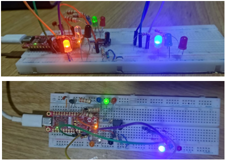
Hardware Implementation
The final prototype showcases an optimized physical implementation, successfully integrating all critical components - including the PIC16F13145 Curiosity Nano, LM35 temperature sensor, and custom IR reflectance circuit - within a compact footprint. This efficient layout minimizes signal interference while providing clear visual feedback through status LEDs.
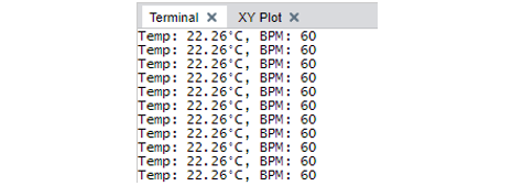
Functional Validation
The system streams real-time sensor data via UART at 9600 baud, viewable through MPLAB Data Visualizer. A critical configuration step requires matching the Visualizer's terminal settings to this baud rate (default is 115200 baud), ensuring proper decoding of temperature and BPM outputs.
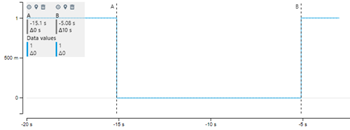
The system’s 10-second sampling interval—critical for accurate BPM calculation—is verified using MPLAB Data Visualizer. As shown below, Timer0’s overflow triggers a precise toggle on RC3 every 10 seconds, demonstrating the reliability of the LFINTOSC clock source and Timer0 configuration.
10-Second Sampling Interval via MPLAB Data Visualizer
System Demonstration
The video below showcases the fully operational prototype, demonstrating immediate visual responses when temperature and BPM exceeds programmed thresholds and the terminal in MPLAB Data Visualizer shows UART outputs displaying both temperature and BPM data. A potentiometer is used to simulate temperature changes.
Resource Utilization
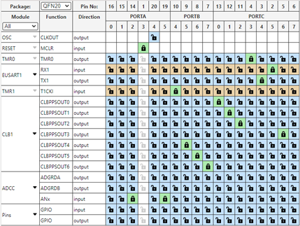
The implementation maximizes the PIC16F13145's capabilities while maintaining expandability. The pin package view reveals peripheral assignments across nearly all available GPIOs.
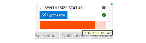
Final CLB synthesis achieved 84% utilization (27/32 LUTs) - a sweet spot between functionality and headroom. This efficient partitioning allows all three detection systems (temperature, pulse, BPM) to operate concurrently while preserving capacity for future enhancements like SPO₂ monitoring.
Amount of LUTs used in this project
Discussion
The project successfully demonstrates how Microchip’s Configurable Logic Block can transform embedded signal processing. By achieving 84% LUT utilization, the CLB simultaneously handles temperature and BPM threshold detection with hardware-level precision—reducing MCU workload compared to software implementations. While the IR reflectance circuit served as an effective prototyping tool, clinical applications would require medical-grade PPG sensors like the MAX30102 for diagnostic accuracy.
Development challenges led to valuable innovations: non-optimized temperature thresholds were resolved through 7-bit truth table simplification, and I²C protocol complexities prompted a creative shift to analog pulse detection. These adaptations highlight the CLB’s versatility in bridging hardware and firmware solutions. The remaining 16% of unused LUTs (5/32) leaves room for expansions such as SPO₂ monitoring.
As a proof-of-concept, the system reveals two key frontiers for embedded health tech: the CLB’s potential to enable FDA-grade devices with proper sensors, and opportunities to integrate actuator control for closed-loop temperature regulation. While currently limited to LED indicators, the architecture’s modular design—confirmed through MPLAB’s toolchain—provides a template for medical IoT innovations.
Conclusion
This project exemplifies how the PIC16F13145 Curiosity Nano’s Configurable Logic Block redefines embedded signal processing. By offloading temperature and pulse threshold detection to hardware, the system achieves deterministic response times using 84% of LUT resources—demonstrating the CLB’s unique ability to blend FPGA-like performance with MCU design simplicity. The successful integration of analog sensors without complicated coding techniques proves the platform’s versatility for mixed-signal health monitoring applications.
Looking ahead, this architecture opens three compelling frontiers:
- Clinical-Grade Upgrades: Replacing prototyping sensors with medical counterparts
- Multi-Parameter Expansion: Adding SPO₂ monitoring via the unused LUTs
- Educational Frameworks: Using the CLB’s real-time processing as a teaching tool for hardware/software co-design
The Curiosity Nano’s CLB isn’t just a peripheral—it’s a paradigm shift for embedded systems. From wearable tech to industrial IoT, this project provides a replicable template for harnessing programmable logic without sacrificing development agility.
Project Resources
The full project package—including schematic PDFs, MPLAB X project files, and CLB Verilog source—is attached to this article for replication and modification. For technical inquiries, contact:
Mateo Sebastián Rojas Flores
[email protected]