A custom PCB platform for learning digital logic using the PIC16F13145 microcontroller. It demonstrates logic gate behavior through hardware-software interaction and helps users explore the Configurable Logic Block (CLB) in practice.
Motivation
While reviewing the documentation for the PIC16F13145 microcontroller, I observed that several assumptions are made regarding the user’s prior knowledge. In particular, it is assumed that the user is already familiar with the behavior of logic gates. Additionally, the available materials lack sufficient detail on how to interface the microcontroller with the Configurable Logic Block (CLB). To address these shortcomings, I developed a Printed Circuit Board (PCB) that serves both as a logic gate demonstration platform and as a support tool for working with the PIC16F13145.
Project Overview
This project aims to provide a hands-on learning platform for understanding digital logic and programming the PIC16F13145. The custom board supports firmware development, interactive learning, and will be accompanied by supporting study materials.
Hardware Design
A custom PCB was developed to bring the concept to life. All design files—including schematics and layout—are available in the project documentation.
Software & Hardware
A custom PCB was developed specifically for this project. All relevant design files, including schematics and layout, are provided in the project documentation.
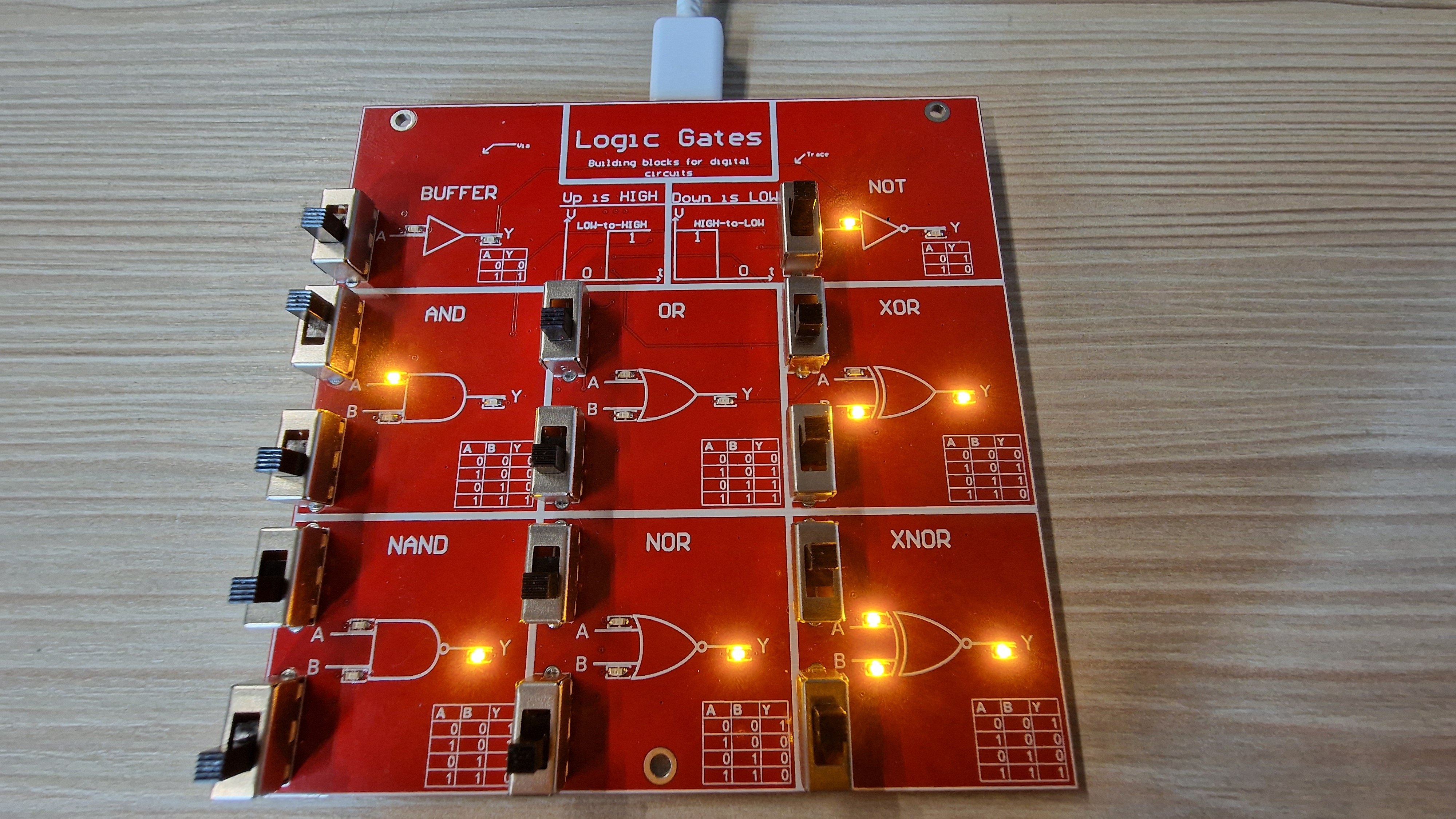
Developed PCB - Front view
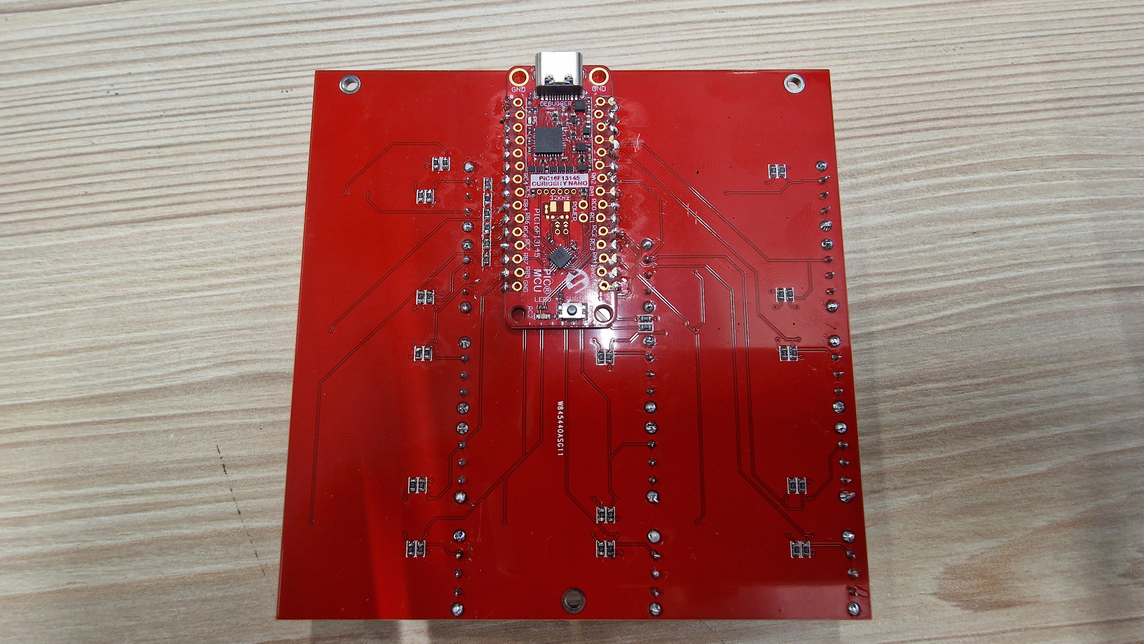
Developed PCB - Back view
Assembly Instructions
To assemble the board, the PIC16F13145 module must be soldered directly to the back side of the PCB. This ensures proper electrical connectivity and mechanical stability for development.
Important Notes
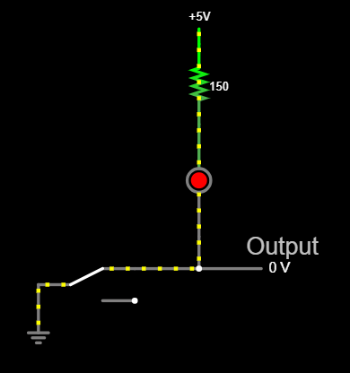
Its cirtical to understand the PCB design for the intented behaviour. The figure below shows how pressing a down switch connects the input to GND (this happens on the real board), allowing current to flow through the corresponding LED. This means the LED will light up when the input is logically LOW. As a result, an illuminated LED does not indicate a logical HIGH — in fact, the microcontroller reads the input pin as LOW in this state. This means that the input HIGH logic is inverted.
#include "mcc_generated_files/system/system.h"

int main(void)
{
    SYSTEM_Initialize();

    while(1)
    {
        CLBSWIN0 = OR_IN_1_GetValue();
        CLBSWIN1 = OR_IN_2_GetValue();
        CLBSWIN2 = NOR1_IN_GetValue();
        CLBSWIN3 = NOR2_IN_GetValue();
        CLBSWIN4 = XNOR_IN_1_GetValue();
        CLBSWIN5 = XNOR_IN_2_GetValue();
        CLBSWIN6 = NAND_IN_1_GetValue();
        CLBSWIN7 = NAND_IN_2_GetValue();
        CLBSWIN8 = XOR_IN_1_GetValue();
        CLBSWIN9 = XOR_IN_2_GetValue();
    }
}
In this loop, each *_GetValue() function reads a digital input pin connected to a specific gate input. These values are assigned to the corresponding CLB switch input registers (CLBSWINx). The CLB logic then evaluates the output in real time, driving the corresponding output LEDs.
When using the CLB to directly read the states of input pins, only four pins can be configured directly into CLB inputs. To overcome this limitation, a software-assisted approach is used: the microcontroller reads the states of all necessary input pins in software and forwards these states to the CLB.
In this configuration, the CLB performs the logical operations (e.g., NOT gates), and the results are then output to the designated pins. This hybrid method allows the use of more than four inputs without losing CLB functionality.
Input side logic inversion. When the LED turns on, the microcontroller reads 0 (logic inversion)
CLB Configuration Strategy
The CLB allows only four direct logic inputs. To overcome this, the microcontroller reads all required inputs in software and sends the values to the CLB. The CLB then performs the desired logic operation (e.g., NOT gate), and outputs the result to the correct pin. This hybrid approach allows for flexible logic design without losing CLB capabilities.
In this loop, each *_GetValue() function reads a digital input pin connected to a specific gate input. These values are assigned to the corresponding CLB switch input registers (CLBSWINx). The CLB logic then evaluates the output in real time, driving the corresponding output LEDs.
For user convenience, each gate’s truth table is printed on the PCB itself, making it easy to verify that the hardware behaves as expected based on the code above.