This project describes my journey when turning a Microchip Configurable Logic Block (CLB) into a driver to generate a signal suitable for serial addressable RGB LEDs containing WS2812B or a compatible chip. Created driver is fully autonomous and does not consume any other peripherals except the clock and interrupt for feeding data to transfer.
Introduction
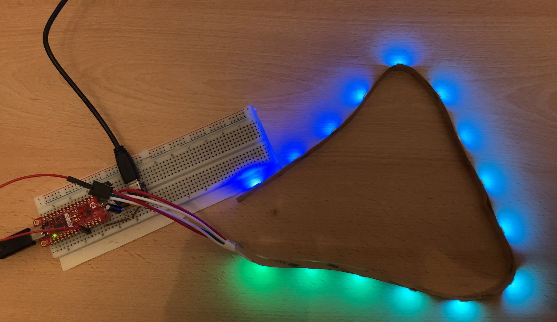
This project demonstrates the implementation of an autonomous WS2812B addressable RGB LED (aka NeoPixel) driver using Microchip's PIC Configurable Logic Block (CLB). Let’s begin by looking at some beautiful RGB Rainbow (outcome of this project):
Usage (TLDR)
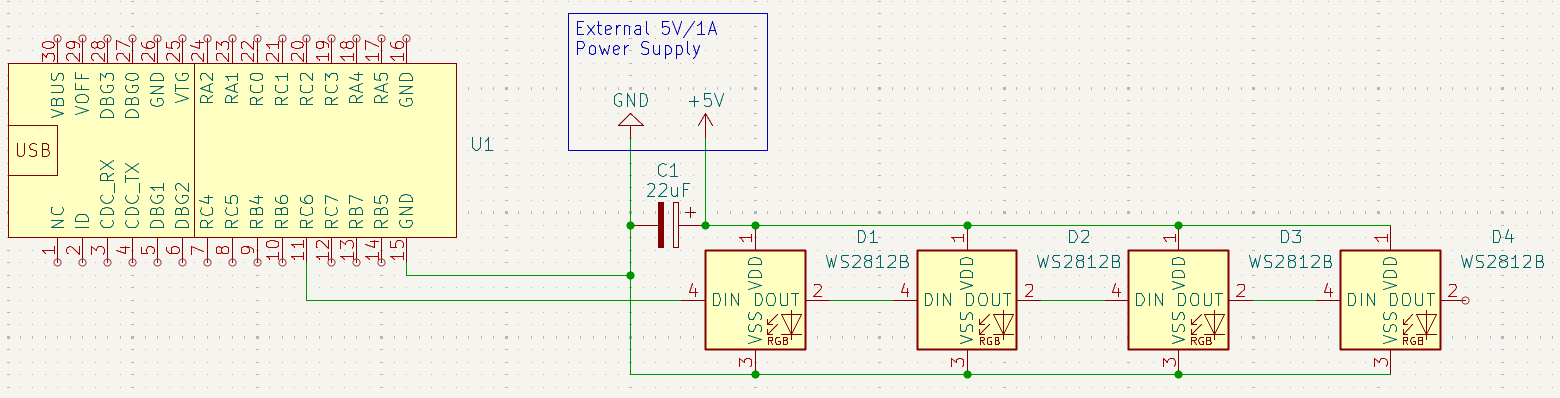
The majority of this article describes the internals of the module, which I implemented and some challenges I faced when designing and implementing it. If you want to just use it, you do not need to read it all. Just go to the end of the article and download the attached project. Then modify main.c file up to your needs. Before flashing the MCU, remember to set Curiosity Nano Board Voltage to 5V by creating a text file with content CMD:5V0 and saving it to the Curiosity Nano storage device (name of file does not matter). Power LEDs using an external 5V supply. Add high capacity (C1 on schematic below) electrolytic capacitor to the LED power rail. Capacity depends on the LED count. Otherwise, LEDs tend to experience brownouts and blinks.
The project is configured to my strip, which contains 15 LEDs. If you want more or fewer LEDs, edit the WS2812_BUF_LEN macro value according to the formula in the comment above it. You can use it with up to 84 LEDs. For more LEDs, it requires a few modifications to the code, but note that it is also limited by MCU RAM, so do not expect much more.
The project is set to map the LED signal to the RC6 pin. In the MCC configurator, you can remap it to almost any other pin you want. The schematic of the demo circuit shown in the video above is as follows:
Schematics of circuit for driving WS2812B LEDs using PIC16F13145 Curiosity Nano Board
Overview of WS2812
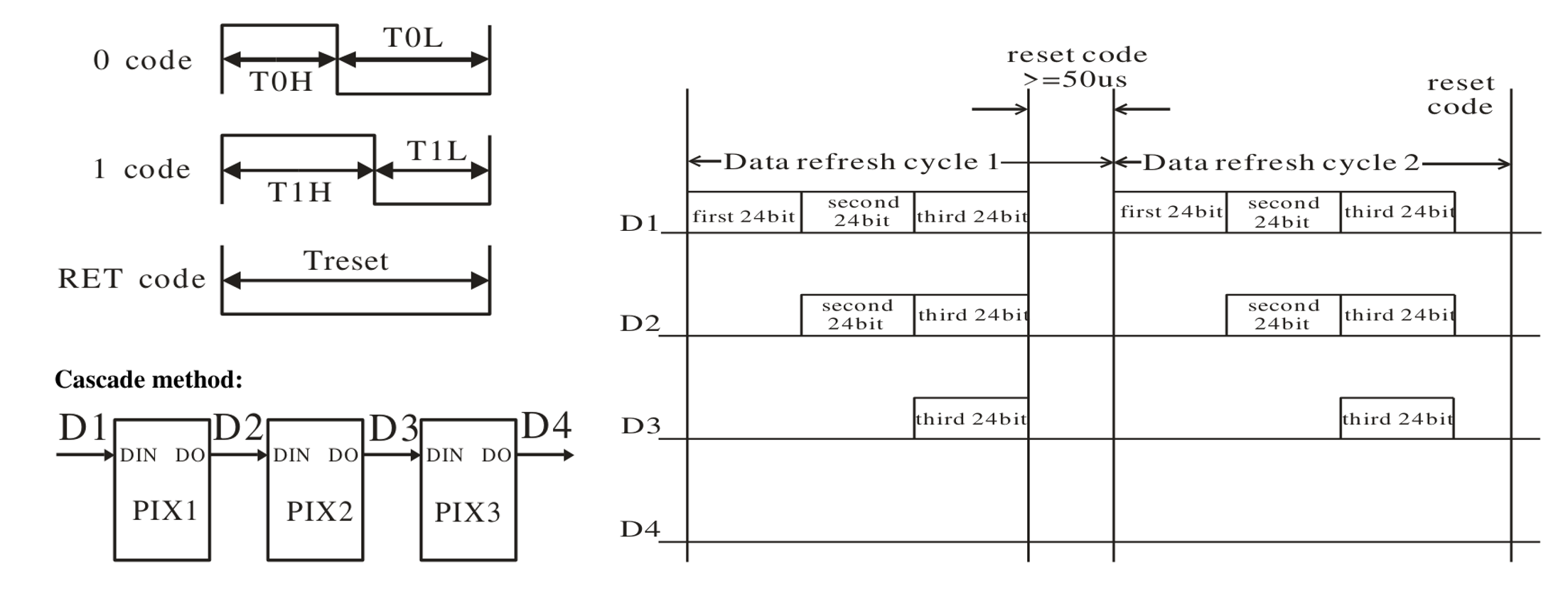
WS2812B LEDs are pretty popular because they allow driving many LEDs using a single pin. They use a pretty unique single-wire serial protocol and daisy chain topology. For every LED in the chain, you send an 8-bit value for each of the red, green, and blue channels (24-bit in total) immediately followed by the data for the next LED. Every LED reads its 24-bit of data, and the rest of the data is forwarded to the next LED. Next LED reads its 24-bit (which seems like the first 24-bit on the bus from LED’s point of view) and forwards remaining data to the next LED. This continues until the last LED receives the last piece of data.
The protocol looks pretty simple at first glance. The bus is low when idle. Every bit is a single pulse on the bus, and the pulse width determines if logical 0 or 1 is transferred. Every pulse is followed by a gap, then the next bit is transmitted in exactly the same way. The datasheet specifies how long the pulse and gap are for each 0 and 1 transfers, and also defines how long the bus must remain idle to consider it as starting a new transmission of the whole chain. Classic WS2812B LEDs require a logical one to consist of a 0.8 us long pulse and a 0.4 us long gap. For transmitting a logical zero, they require a 0.4 us long pulse and a 0.8 us long gap. To consider restarting the transfer from the start, the bus should be idle for at least 50 us. WS2812B LEDs were cloned several times. You may find similar LEDs with slightly different timing requirements. Here are some pictures from a typical WS2812B datasheet:
WS2812B Timing Diagrams from Datasheet
Driver Implementations
There are several techniques for generating such a signal, but interestingly, all have some pros and cons. Implementation typically utilises the shape of the format. 0.8 us is exactly twice 0.4 us, and every transfer is equally long, no matter if you transmit logical 0 or 1. Every transmission begins with at least 0.4 us of logic 1 and ends at least 0.4 us of logical zero. The remaining 0.4 us in the middle is defined by the bit you transmit. If you transmit 0, the middle part is logical 0 and similarly for 1.
In the old days, the typical solution on slow Arduinos was to disable interrupts and then bit band the signal. Because the signal is pretty fast (0.4 us period equals 2.5 MHz frequency), it was typically implemented in assembler and code was filled with precisely tuned numbers of nop instructions to achieve the desired bus timing.
In the case of modern high-performance MCUs, there are more options. Some people realised that if your MCU can do SPI transfer without gaps between bytes, you can encode a 1-bit transfer as 3 bits of data and transfer it using the SPI peripheral (clocked at the right frequency) while using only the MOSI wire.
In even more modern MCUs, the requirement of gap-free SPI transfers was typically achieved using DMA, which also allows the CPU to spend time on more useful tasks while generating an LED signal in the background.
A common drawback of implementation using modern MCUs is the requirement for a 2.5 MHz frequency, which is not very common. Typically, you easily have 1 MHz, 2 MHz, 4MHz, 8 MHz, 16 MHz, etc. But you very rarely have 2.5 MHz. Similarly, you very rarely have (possibly prescalable) multiples of 2.5 MHz because 5 MHz, 10 MHz, and 25 MHz are also not very common. So, in practice, you need an integer prescaler or a very highly configurable PLL. In advanced MCUs, you typically have these, but it forces you to waste these valuable resources on things as simple as driving LEDs.
Let’s sum it up. For driving LEDs like WS2812, you typically need
1. Waste CPU power on bit-banding and block other application duties completely in that time
2. Waste SPI peripheral just for driving LEDs
3. Waste DMA controller just for LEDs
4. Constrain the clock system of the whole application based on LED clock requirements
Or maybe, you just need a CLB?
The implementation which I describe in this article tries to minimise these requirements as much as possible. It will not require blocking the whole CPU when transmitting data on the LED bus. It does not need SPI and DMA. It can also work on an 8 MHz clock (or any which can be prescaled to 8 MHz).
Microchip’s CLB Example
Microchip has already implemented the WS2812B driver using a peripheral named Configurable Logic Block (CLB) for you. CLB is a configurable array of logic gates which you can reconfigure with your small logic circuit. Microchip's design of WS2812B controller utilises a SPI controller and CLB to post-process its output. This solution works, but you waste the SPI peripheral, and you are required to run the SPI peripheral at the required frequency.
But since CLB is pretty flexible, I thought that I could do it better than Microchip did. The idea which I had in mind was to make it fully implemented in CLB without dependency on any other peripheral except some basic clock and interrupt, which the firmware will use to feed data to the peripheral.
Resource Effective Fully CLB-based Driver Journey
Before I got PIC16F13145, I prepared some drafts of the design which do not depend on any other PIC peripherals. It is nice that you can use the CLB configurator tool online in a browser, even without having access to HW. My original design fit the capacity of CLB (which is 32 logic elements) and utilised about 75% of resources.
Designing a CLB circuit without access to HW is nice, but when I got a PIC16F13145 Curiosity Nano board and tried it on real hardware, I found that it does not work at all. I made a few mistakes which I had to fix, and I had to redesign a few parts from scratch. The final circuit fits it very tightly. It uses 100% of the CLB resources. At the end of the design phase, it was pretty painful because when you are reaching CLB limits, you likely overflow them at some point and get synthesiser errors, which I regularly got. It is even amplified that sometimes even slight changes in the circuit change the number of used resources a lot. Even small changes like changing output pin from one to another, swapping input pins, switching IRQ0 to IRQ3, ..., can influence the number of used resources. When you are at the resource usage limit boundary, all these small changes can prevent your design from fitting. So, if you want to play with my design (which is attached at the end of this article), pay attention to this. The circuit is very tuned.
Now, let’s see how my circuit works.
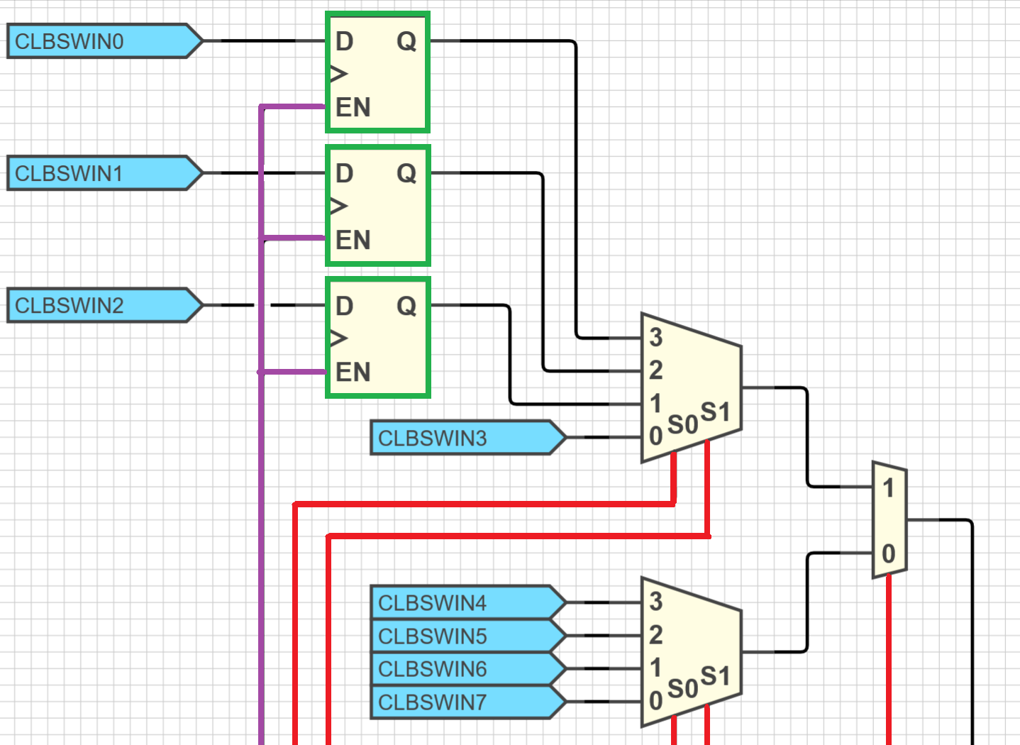
CLB Diagram
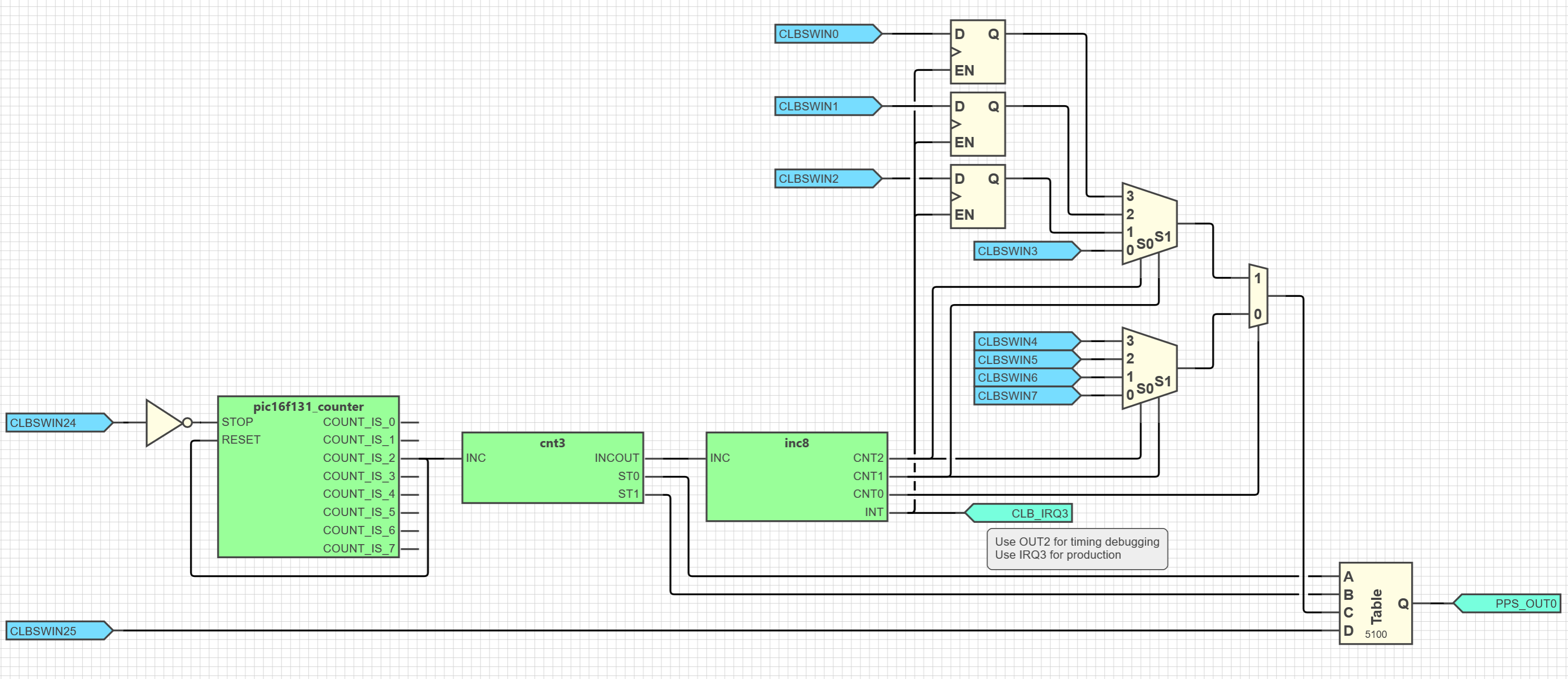
CLB Block Diagram of my WS2812B signal generator peripheral
It has 10 inputs and 2 outputs. 8 bits of input are a register for passing data from FW to the driver. The remaining two bits are control bits which enable transmission and enable transmission of reset mode (making the bus idle). One output is the signal to the LED chain. The second output is an interrupt signal which triggers the interrupt service routine in the CPU.
There are three green blocks which contain some helper automata inside.
The first one (from left to right) is easy. It is a 3-bit timer which is embedded in the CLB. It is fixed control. I use it for integer division of frequency. CLB, as designed, runs using a 32 MHz High Frequency Internal Clock (HFINTCLK), which is prescaled by 4 to 8 MHz. This counter counts three steps, and at the third step, it generates a pulse which is connected to the circuit. These pulses happen 3x less frequently than pulses of the input clock happen, so it efficiently divides an 8 MHz input clock by 3 to a 2.66 MHz frequency. This is near enough (in tolerance) to the frequency we need. As you can see, the timer is enabled/disabled by a control bit driven by firmware. It resets when it reaches the third step. Reset happen at the same time, when it generates a pulse for the application.
All inputs to the circuit come from the CLBSWIN register, which is the channel MCU can communicate with the logic circuit on the CLB. MCU can write this register, and the data appears in the corresponding input signals in the CLB.
The second block is my customised counters. It is a 2-bit counter, but it does not count from 0 to 3. Instead, it counts only up to two. Then it resets to 0. Counter value is available on the ST0 and ST1 outputs. This counter generates state information on what part of the bit transmission is currently ongoing. Remember that every bit transmission to WS2812B consists of 3 parts: a fixed logical 1, a bit depending on the transmitted data, and a fixed logical 0. The state of this counter is then processed by the final look-up table (the rightmost control on the diagram before output).
Additionally, this counter generates a short pulse (referred to as INCOUT) at the beginning of the third state. Remember that the bit value is transmitted in the second state, so this pulse happens right after the bit value transmission is done, and the bit value is no longer needed. This pulse causes the bit selector to select the next bit.
Before I describe the last green block, let’s look at the already mentioned bit selector first. It is a circuit consisting of 3 multiplexers:
Highlight of bit selector part of CLB block diagram.
Multiplexers select one of their inputs based on control signals (they are highlighted red on the picture above). The control signals for selecting bits are three. They choose one of the 8 bits to transfer. After the bit transfer is done, control signals change (this is driven by the last, not yet described, green control block), and they start selecting the next bit. Bits are transferred from the highest (7) first to the lowest (0), which corresponds to how WS2812B LED expects data.
CLBSWINL is an input register loaded by LED signal data by the firmware. As you can see, there is one interesting thing. Bits 0, 1, and 2 are not directly connected to the bit selector, but they are connected using DQ cells, which are highlighted by green borders and the diagram above. This is, btw, the part which I omitted when making the original prototype in the browser. This cell makes the lower three bits (the bits which are sent last) of the CLBSWIN register double buffered. Double buffering means that these cells hold the same data as they were in the register when the EN signal (highlighted purple on the image), even after the register gets overwritten by new data. This is very important. If this register were not double buffered at all, the MCU firmware would need to load new data after the last bit is transferred and before the first bit of the next data is transferred. If it loads data sooner, then transmission of the last bit would be corrupted (because it would contain a bit overwritten by the bit from the newly loaded byte, which contains data for the next transfer). Similarly, if firmware writes data here late, the first bit of the next transfer will be corrupted (because it would contain a bit from the previous transfer, which was not overwritten yet). Double buffering solves that. When the 5th bit gets transferred, the EN signal is triggered. Note that the EN signal is the same signal which goes to the MCU interrupt. So, while MCU receives a request to load new data to register, the register gets buffered at the same time. The circuit will continue transmitting the data which were loaded there at that time, but the MCU is now allowed to load new data. Now the MCU have a pretty long time to load data. It still needs to do it before the first bit of the next data starts transferring, but now it has a time budget equivalent to the transmission of 3 bits. This is much better than needing to load them exactly between the end of the last bit and the start of the first bit. The double-buffering mechanism makes timing requirements less strict, which is important because there is still a pretty lot of work on the firmware side. Firmware needs to load the buffer pointer, compute the address of the element to load, check if the buffer is exhausted and prevent buffer overflow, load new data or stop the peripheral, increment buffer pointer for next transmission, ... . Despite double-buffering weaken timing requirements, I still had to optimize firmware a lot. I will describe this later in the firmware section.
Ideally, all 8 bits should be double-buffered. In that case, immediately after the transmission of the byte begins, the MCU can load new data for the next transmission while having the time budget of the whole transmission cycle to complete this operation. But unluckily, I reached 100% utilisation of CLB resources. Instead, I had to optimise the MCU firmware to achieve loading data fast enough for 3 double-buffered bits.
Well, and now we are at the last green block. It is the counter which drives the bit selector. When it receives a pulse from the 3-state counter, it changes the selection signal to select the next bit to transfer. When it increments from the last non-buffered to the first double-buffered bit, it also generates an interrupt signal, which indicates to the firmware that it is the best time to load data for the next transmission.
The last part, which was not fully described yet, is the last LUT which generates the LED signal. Input D is directly connected to the control register. This bit enables reset mode, which continuously generates a low signal for the remaining bus in the idle state. Once deasserted, it starts generating pulses based on a 3-state counter, which is fed to inputs A and B. Input C is a bit value from the bit selector, and this value is promoted to the bus in the middle of the 3-state transfer.
And that’s it. All parts of the circuit are described. Let’s briefly describe how firmware controls this engine and what challenges I faced when implementing it.
Firmware
Since the majority of complexity is hidden in HW, firmware is pretty simple. But still, some parts of the firmware are tricky, mainly because of performance optimisations needed to achieve loading data to the peripheral within the time frame of 3-bit transmission, which is double-buffered. The firmware part controlling CLB consists of only 3 functions. The first function, WS2812_SetLed, simply loads R, G and B for the specified LED. It sets an internal buffer in the MCU RAM, but does not issue anything on the bus. WS2812_Transmit configures the peripheral and starts transmission, and finally third function is the most important one. It is an interrupt handler which drives the transmission process.
For minimising interrupt latency, I had to write __interrupt() attributed interrupt handler instead of using handlers generated by MCC, which contains several indirections, which slowed the program to the level that loading new data to the register happened too late, and the device was transmitting corrupted data. For a similar reason interrupt handler is highly optimised to load data into the register as soon as possible.
Firmware stores LED data in a contiguous buffer in RAM (WS2812_SetLed() writes this buffer). The capacity of this buffer is defined by the macro. The more LEDs you have on the bus, the bigger buffer you need. The LED data buffer is in RAM. While device RAM is limited (1KB in the case of PIC16F13145, which I use), the number of drivable LEDs is also limited. Designed firmware supports up to 256-byte-long buffers, which efficiently brings support for up to 84 LEDs.
Now let’s look at how firmware loads data to hardware and how it synchronises with it.
Loading Data to CLB
The most interesting part of loading data is performance optimisation. Because the LED bus is pretty fast and the register has only 3 bits double buffered, the firmware needs to load data on an interrupt very quickly. For this reason, it is almost first operation which happens in an interrupt. The first action is checking and resetting the interrupt flag. Data load happens immediately when the flag is detected and cleared. To make it super fast, some operations are in reverse, unintuitive order. One example is an intended buffer overflow. To load data as soon as possible, the firmware first loads data to the peripheral and then checks that there is enough data in the buffer. Normally, it should be done in reverse order (first check, then access memory). Such incorrect order causes a buffer overflow, which actually reads exactly one byte after the buffer boundary. To make this intended buffer overflow safe, the buffer is one byte longer.
Actually, there are two reasons for the buffer being one byte longer: the first is already mentioned. We compare the read pointer after reading from it, so we need it to make a one-byte buffer overflow safe. Second, my circuit in CLB does not provide any information or logic for stopping the transfer at the right time. Remember that an interrupt is generated between the 5th and 6th bit transfer. Even at the time of the first interrupt after transmitting the last byte get transmitted, device can’t stop the peripheral because the interrupt happens between the 5th and 6th bit, so the remaining 3 bits still remain to transmit, and the device does not know when it exactly happens. For this reason, the buffer is one byte longer, and the device initiates one more transmission of dummy data. After this happens, the device can close the peripheral on the next interrupt, knowing that if it breaks some transmission soon, it is not an important transmission because it is definitely an intentionally overrun byte.
Transmitting more (dummy bits/bytes) (after useful data transmissions are done) is not a problem on the WS2812B bus. After all LEDs are loaded with data, the LEDs continue the process. They forward dummy overrun bits. At some point, the firmware cut it by stopping the peripheral. The point when the firmware stops is a random moment of time within the byte transmission, so it actually emits a non-deterministic number of pulses. Actually, it is fully deterministic. It just depends on firmware execution speed, so unless you write in assembler and count clock cycles, you should not rely on it. But for LEDs, it is not a problem. They forward bits of this last byte over the whole chain up to the last LED. The last LED is already loaded at that time, so it forwards it further. But because there are no more LEDs after the last one, nothing processes the garbage. After the transmission of dummy bits is done, CLB is shut down, and the bus stabilises at the idle state, and each LED resets its controller and waits for the next round of data.
Reset Generation
Device and firmware contain logic for generating a reset condition (bus hold low for at least 50 us). Technically, it is not necessary to support it as long as the user firmware waits at least 50 us before starting a new transmission after the previous transmission is done. But since adding support for it was easy on the hardware side, I added it there. Simply, there is a control bit which allows to whole peripheral at the background but bypasses it and generates a logic low signal. Firmware starts transmission in this mode. It runs several cycles (defined by the C preprocessor macro) of this process, which holds the bus low long enough. After it finishes a specified number of these cycles, it turns this control bit off and starts data transmission. But well, because of some simplification in synchronisation, it is not that easy.
Switching between Reset Generation and Data Transmission Mode
The problem is again that firmware does not know when the transmission starts/completes, so if it releases the reset mode control bit at a random time, it will start immediately outputting part of the transfer which was running in the background and was suppressed by the reset mode. Instead, firmware utilises the CLB state clearing behaviour. Disabling and re-enabling CLB is one way to clear the state of all logic elements back to zeros. This causes all 3 state machines to reset to their initial state and sets them to a deterministic state. After the peripheral is re-enabled with reset generation control bit disabled, it starts transmission from the first bit as expected. This is a reason why firmware contains parts which disable CLB and almost immediately reenable it.
Demo Application
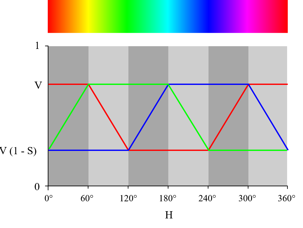
Demo application which I prepared to demonstrate my controller contains logic for computing a rainbow animation. It generates a rainbow animation using the pattern described on the Wikipedia page, using this diagram:
Schema of color transitions when generating rainbow pattern
Each LED is slightly shifted, and the whole animation iterates continuously. The amplitude of the pattern as well as the timing is configurable using a C preprocessor macro. Here is the animation. Mobile camera has a hard time recording such bright LEDs properly. In real life, colours are brighter and more colourful:
Evaluation
And here we are. Let’s evaluate my design. It satisfies the original requirements. It generates WS2812B compliant signal and does not depend on any other peripheral except the clock and one interrupt for loading data to transmit. It does not require you to waste any timer for generating a reference clock, and it does not require you to waste any SPI or DMA to generate a bit pattern. All these peripherals remain in the PIC MCU for another use in your application. The circuit designed by me contains a minimalistic implementation of all these directly in the CLB. The device utilises all 32 of 32 logic elements offered by CLB, so with this circuit, you can feel good that you utilised every cent you paid for CLB in your PIC. In opposition, if you decide to extend or modify my circuit, you will have a very hard time. While there are a few hacks, like one-byte intended buffer overflow, the device works well and reliably. As a drawback, I consider pretty strict timing requirements on the interrupt handler, which make it hard to read and understand and also limit application usage of other interrupts when LED data is transferred. But compared to the old AVR soft implementation, firmware does not need 100% CPU dedication to LED handling, and you can keep your program running at the time when data is transferred. Peripheral will interrupt your firmware regularly, but between interruptions, your program runs without any limitations.
Summary
Thank you for reading up to the end. In this article, I described my WS2812B controller, which I implemented using the Configuration Logic Block feature of the PIC16 microcontroller, which runs without depending on any other peripherals, which makes it a pretty unique implementation different from what you can find in Microchip CLB samples. Feel free to download and test it below.