Using TPS25730SRSMR to generate continuous 12V from a USB-C PD supply for projects.
While this device could be used for any application, I had a need for a +12V/-12V PSU to use with an analogue synthesiser. The synth uses opamps connected to a dual rail supply in order to drive speakers at their maximum power.
Requirements:
- Steady DC +/-12V output (Max. 2A)
- USB-C so any standard PD charger can be used
- Output via screw terminal for easy prototyping
- Output via 35mm jack for use in synth system
Design Specification
Component Selection
I chose to go with a Texas Instruments device for known reliability. Using their website USB Type-C & USB Power Delivery ICs product selection | TI.com I identified the TPS25730SRSMR chip would be suitable. This is readily available, less than a dollar, and supported up to 20V output. Some PD chips only support up to 5V or only work for sourcing power and not sinking it like I need.
The TI datasheet for TPS25730SRSMR also includes a very detailed set of Application Notes which detailed exactly how to use the IC and example circuits/PCB layout.


Schematic Capture
For this project, I wanted to learn how to use EasyEDA for both the schematic capture and the layout.

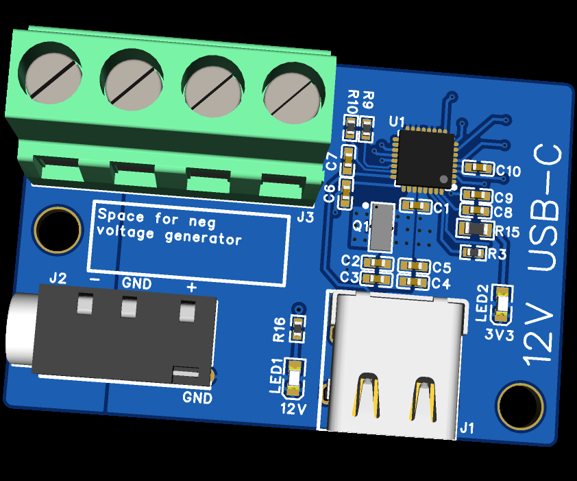
I copied the BOM of the application note and added the USB-C connector J1, as well as LED1 and LED2 to act as power indicator LEDs. For easier understanding I have outlined each section of the schematic with a pink box and heading, with calculation notes next to the components where relevant.
To select 12V as the target output voltage from a PD supply, I used the datasheet to adjust the ADCIN values.

Where the potential dividers are calculated as:

So the following resistor values were chosen to get 12V @ 2A from the PD supply.
Layout Capture
As recommended in the datasheet, I have used a 4-layer PCB for this prototype. There is not much to say about the design of the layout because the design is copied from the application note, including the placement of vias. The additional components, mainly the USB-C connector, had to be carefully routed around the existing components.

Top = GND
Inner1 = Supply
Inner2 = GND
Bottom = GND
There is also a copper pour on the top left for the negative voltage output. This is ready for future development as the negative voltage has not been implemented yet.
Connectors J2 and J3 will be used to output the power to other devices, either with a 35mm audio jack or a screw terminal block. They are also set far away from the control circuitry so they can be connected to the negative output when this is implemented.
Manufacturing
After I was happy with the layout, I exported the BOM and the Gerber files so that a PCB manufacturer would be able to produce the physical hardware. PCBWay were kind enough to sponsor this project for both the components and the assembly of the boards, so thank you.
I used the Gerber uploader to get my design into their system and selected the correct parameters (board layers etc.). I also checked the box for assembly which prompts you to state how many unique components will be assembled.

I was then able to upload the BOM and pick and place files for accurate quoting.

After this stage I felt that I received a very professional service. I had a single point of contact at PCBWay who verified the design files and BOM, sending me a list of alternative components that I had to approve before they started production. The website was super clear on the progress of the bare board and assembly, giving a timeline to the second on which stage was being worked on.
I can definitely recommend using PCBWay for large scale productions due to the ease of re-ordering, as well as the ability to sell your designs on the site to other users.
Testing
The boards arrived very well packaged in ESD bags and arrived very quickly after they were assembled.

I checked the boards over in a basic visual inspection before powering up the devices.

When I plugged the board into a power supply, the 12V LED would blink, indicating that the PSU was entering some kind of hiccup mode. The TPS chip was clearly outputting power, but not steadily. I measured the output with an oscilloscope to confirm that it was reaching 12V, and even when changing the PSU the power would continue to hiccup.

I also observed that the 3V3 LED would not light up, which gave me more cause for concern. At this point, I went through a deeper dive of the datasheet and found that this 3V3 line does not come from the USB but from a battery on the device (clearly assuming the connected device will be charged and used wirelessly). Meaning this is not a useful debugging tool for my application.

I did connect the 3V3 line to a bench top PSU to see how it affected the system. When connected, LED2 would light up but the high voltage output from the chip was no longer present, even in hiccup mode. This further highlighted my misunderstanding of the PD chip I had selected.
I did not come to a conclusion as to why the board was not functioning as expected.
Next Steps
My first action will be to replace the basic components with the same as those in the application note. While this won't meet my initial specification, it will confirm the operation of my board against a known working system.
Once I have achieved this, I will re-visit the ADCIN potential dividers to confirm that the target voltages/currents are achievable with the power supplies I have available for testing. I may have miscalculated the values needed for my target voltage.Unfortunately I have not discovered a way to simulate these ICs so will need to order more boards when I think I have resolved the issues.
The final step, once the basic operating has been fixed, is to implement a negative voltage rectifier on board so that I can use this power supply for dual rail op-amp circuits.