This project presents a low-cost AC-DC converter for low-power always-connected applications.
Below we described steps needed to understand how the solution has been programmed to create the AC-DC converter. However, if you just want to get the result of programming, download GreenPAK™ Designer software to view the already completed GreenPAK Design File. Plug the GreenPAK Development Kit to your computer and hit the program to design the device.
Modern devices have driven the need for compact, low-cost off-line regulators. Off-line regulators which use inductors are efficient but are often large and costly. This project will describe how to implement a circuit that instead uses a capacitor-coupled switched shunt regulator controlled by a GreenPAK SLG46110. This circuit can provide a low-cost AC-DC converter for low-power applications such as smart lighting.
Operation Principle of CCSS Topology
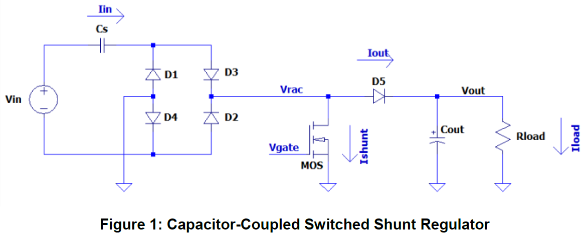
At a basic level, shunt regulators consist of two elements: a voltage regulator in parallel with the load (shunt) and a current-limiting element in series between the supply and load. The shunt regulator used in this project is specifically a capacitor-coupled switched shunt (CCSS) regulator (Figure 1). When the switch is closed, it short circuits the input current to ground. When it is open, diode D5 diverts the input current to the load. Besides the series capacitor (Cs), the highest voltage seen by the other components is one diode drop above Vout.
As with all shunt regulators, input current to a CCSS regulator is constant regardless of load but varies with input voltage and the series capacitance. Although current will always be drawn even under no-load conditions this current is mainly reactive with a small real. Input current can be estimated with the following equation:
??? = ??? / ?c
Output voltage regulation is achieved by controlling the duty cycle of the switched shunt. The MOSFET shunt turns off when the Vout is below the desired regulation threshold, sending all the input current to the output. When Vout exceeds that threshold, the MOSFET shunt turns on, sending all the input current instead to ground and back to the input. The shunt is synchronized to turn on when the voltage across it (Vrac) is low to minimize the applied voltage step across Cs resulting in a more efficient operation.
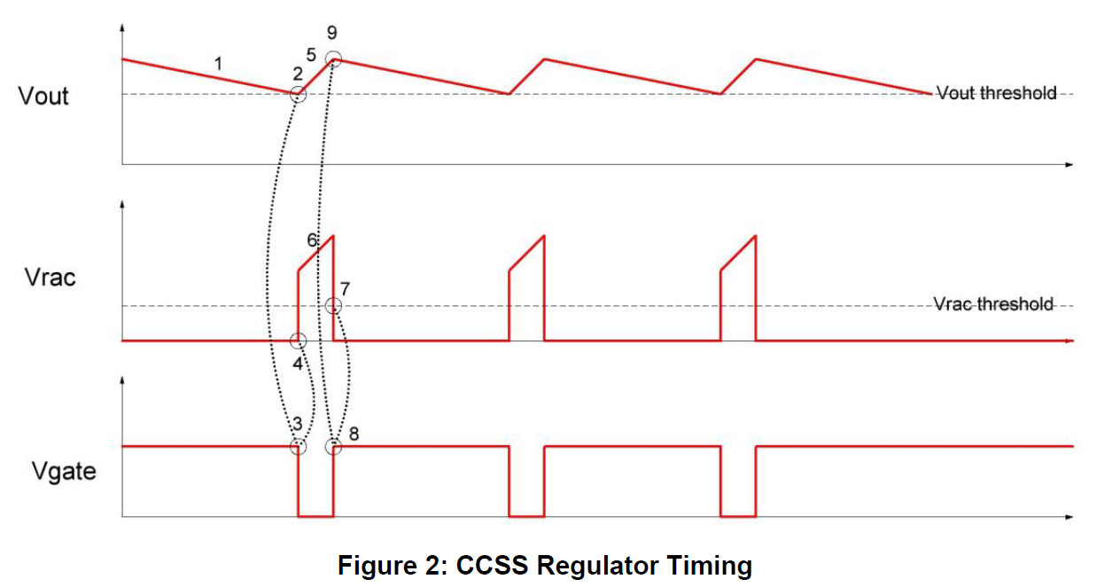
The following diagram shows the operation of this control manner from a timing perspective.
Figure 2 describes the CCSS timing diagram:
Output voltage decays under load until
It hits the Vout threshold which
Turns off the shunt
Freeing the Vrac from GND
Vrac is clamped by D5 (Vout-0.6V) when Vout starts to rise until
Vrac falls below Vout as AC input
Vrac falls to Vrac threshold …
The shunt is turned on, Vrac is clamped by GND …
Output voltage decays under load and the cycle repeats.
The MOSFET cannot turn-on immediately when Vout exceeds the threshold, which results in overshoot at the output. A larger capacitance for Cout or operating the regulator over a narrower input voltage range can minimize the overshoot.
Circuit Schematic and Layout
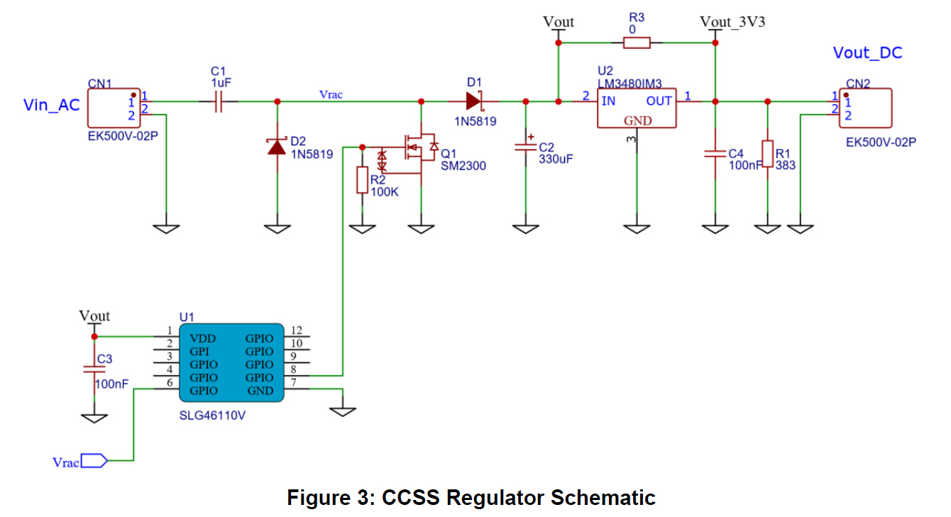
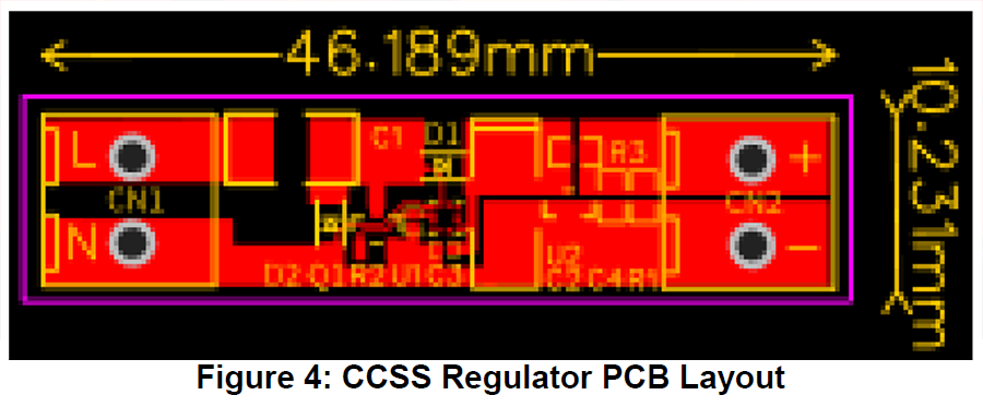
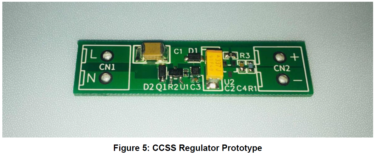
Figure 3 depicts the circuit schematic of the low-power AC-DC converter module. It uses the SLG46110 (U1) to control the CCSS. The module operates at an input AC voltage range from 90V to 260V(CN1), and over a non-isolated output of 3.3V (CN2). An optional LDO (U2) is added after the Vout to further stabilize the output voltage. The SLG46110 device generates the control signal that switches the MOSFET shunt (Q1) based on the Vout and Vrac threshold levels. 1N5817 Schottky diodes were used for D1 and D2. Since the dissipation factor (DF) of CS has a large effect on the efficiency of the circuit, a 1µF capacitor with a relatively small DF of 40 x 10-4 is used for CS. Figure 4 shows a picture of the PCB Layout of the board. Figure 5 shows a photograph of the complete design PCB described in this project.
GreenPAK Design
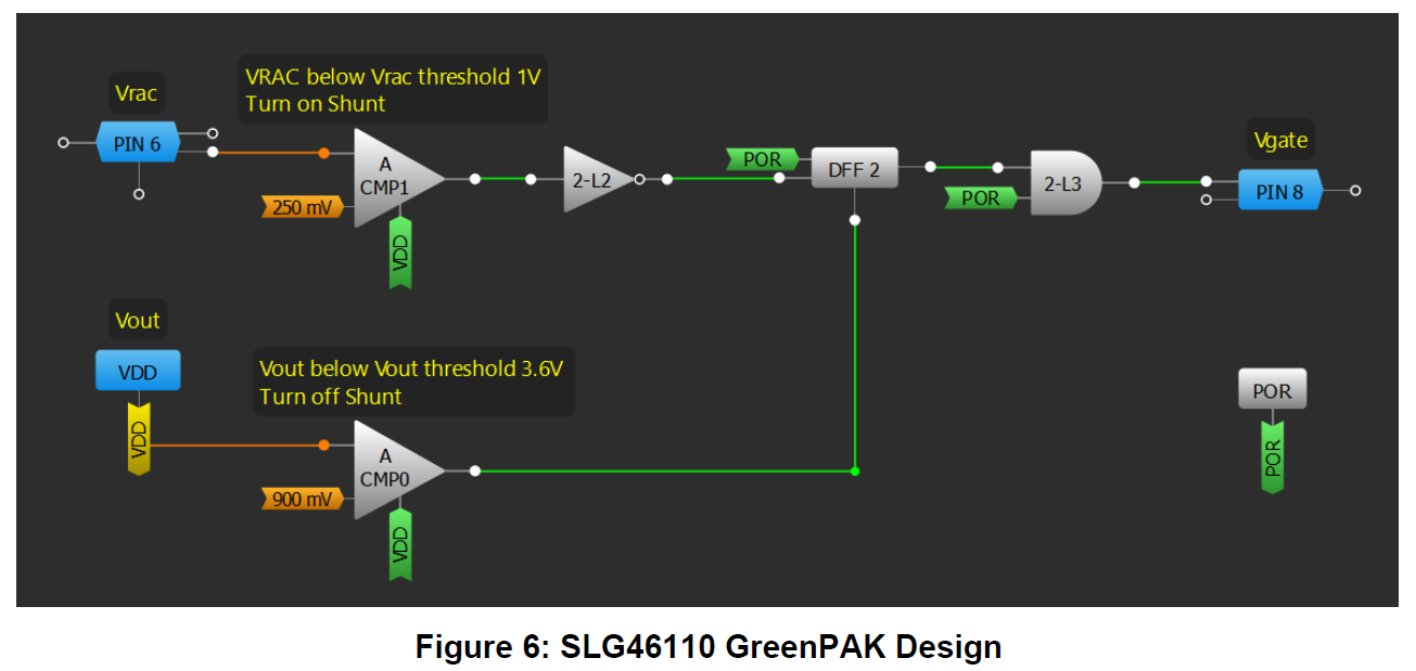
The project design developed in GreenPAK Designer is shown in Figure 6.
Comparator Configuration
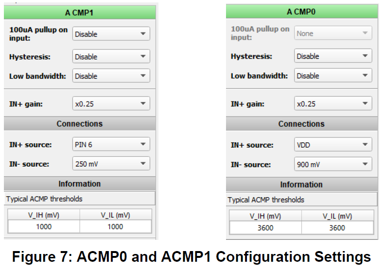
As shown in Figure 3 VDD of the SLG46110 device is connected to Vout and PIN6 to Vrac. ACMP0 is used to sense Vout voltage. With the additional logic, it will turn off the MOSFET shunt when Vout < 3.6V. ACMP1 is used to sense Vrac voltage. It will turn on the MOSFET shunt when Vrac < 1V. Refer to Figure 7 for the ACMPs settings.
Measurements
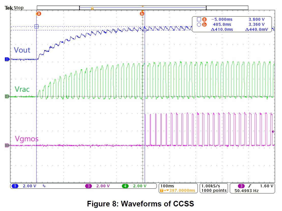
The module is tested at the 150 V AC RMS input voltage. The gate voltage of the MOSFET shunt and the output voltage signal is measured. Figure 8 displays their waveforms. The ripple of the output voltage is about 440 mV.
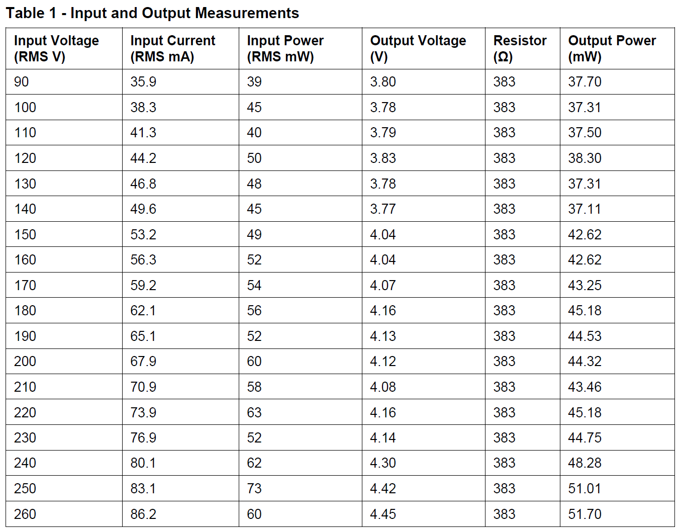
Below in Table 1 are the input and output measurements. The input RMS power is calculated with an AC power meter and the output power is calculated by multiplying the output voltage by the squared value of the resistor. As stated previously, Cs is a 1uF capacitor with a DF of 40 x 10-4.
Conclusion
This CCSS converter provides a compact, low-cost inductorless alternative to a typical AC-DC converter system, which is ideal for low-power applications. The GreenPAK has additional logic and GPIOs available which gives the flexibility to include additional functions to its switching control without buying another device. The switching circuit can be implemented in any GreenPAK with two ACMPs, so a different GreenPAK with the desired functionality could replace the SLG46110. For instance, an SLG46140 could be used instead to provide PWM control to an LED light.