Custom
Clocked JK Flip Flop: Complete Guide with Circuit, Truth Table, and Working
RT
October 25, 2025 by Rinme Tom

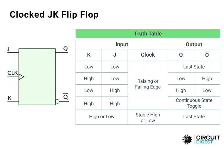
The JK Flip-Flop is a universal digital memory circuit widely used in counters, clock dividers, and control logic. Unlike SR, D, or T flip-flops, the JK design eliminates invalid states and allows toggling functionality, making it ideal for modern electronics. This project explores the construction of a clocked JK Flip-Flop using NAND and NOR gates
Scroll to continue with content
Project Objective
Build a clocked JK Flip-Flop using six NAND gates, demonstrate functionality for all input conditions (set, reset, hold, toggle), and showcase applications in counters and frequency dividers.
Key Features
- All input combinations (00, 01, 10, 11) are valid and predictable; no forbidden states.
- Toggle function when both inputs are high, enabling frequency division and counting.
- It can be configured as an SR, D, or T flip-flop, offering design flexibility.
- Edge-triggered operation, responding only on clock transitions for reliability.
Circuit Details
- NAND and hybrid NOR gate implementations are presented, with six 2-input NAND gates in the classic build.
- Logic diagrams, truth tables, and wiring instructions guide the practical assembly.
Applications
- Binary digital counters, frequency divider circuits, shift registers, and memory units.
- Integrated solutions (like the 7476 and 74LS76 ICs) simplify larger digital system designs.
Troubleshooting and Tips
- Common issues like erratic output or state toggling problems are outlined, with solutions such as signal integrity checks and proper wiring references