This project shows that the GreenPAK ICs can implement a room thermostat thanks to its flexibility and configurability.
A thermostat is a device which senses the temperature of a system and automatically regulates it so that the temperature of the system is maintained near a desired setpoint. It is a closed-loop control device, as it seeks to reduce the error between the desired and measured temperatures. Room thermostats usually have a working range of 5°C to 30°C, and they can work in either heating or cooling mode. They also have a display to show the user information about the room's actual measured temperature and desired set temperature. These requirements make the GreenPAK SLG46620V suitable for designing a simple room thermostat.
Figure 1 depicts the high-level system design of the implemented thermostat.
The system is composed of the following components:
- Power supply unit (input 24VAC, output 5VDC)
- Thermistor MCP9700A (temperature sensor)
- Potentiometer – used for setting the desired temperature
- 2-digit 7-segment display – used for displaying current and set temperature
- Pushbutton for mode select (cooling or heating)
- Pushbutton for displaying the set temperature
- Relays
- Relay Drivers
- GreenPAK SLG46620V
Below we described steps needed to understand how the solution has been programmed to create the room thermostat. However, if you just want to get the result of programming, download GreenPAK Designer software to view the already completed GreenPAK Design file. Plug the GreenPAK Development Kit into your computer and hit the program to design the device.
1. Top Level Design
1.1. Power supply unit (PSU)
Room thermostats available in the USA are supplied with 24VAC. System logic, relays, displays, and temperature sensors have a working voltage of around 5VDC, so we need to design and implement a power supply unit (PSU) which will have 24VAC input and 5VDC output. This PSU is based on a MC34063 switching regulator. Figure 2 depicts the electrical schematic of the PSU.
1.2. Temperature sensor – MCP9700A
The MCP9700A is a linear active thermistor which converts temperature to voltage with following features:
- Small size
- Wide temperature range -40°C to +125°C
- Precision ±2°C(max.) in 0°C - 70°C range
- Optimized for analog to digital converters 10.0mV/°C output
- Voltage supply range VDD=2.3V to 5.5V
- Low current consumption, 6µA
- Vout=500mV for 0°C
Compared to thermistors, a linear active thermistor does not need an additional circuitry for signal conditioning, and it can be directly connected to the input of an ADC.
Figure 3 shows that the output voltage from the MCP9700A temperature sensor is linearly dependent on the surrounding temperature.
1.3. Thermostat design
Figure 4 shows the thermostat design. An analog voltage comparator is used to compare the desired temperature and temperature measured by the MCP9700A sensor. A potentiometer is used for setting the desired temperature.
The middle output from the potentiometer is connected to the input of the analog comparator.
Figure 5 shows the principle of operation for the analog comparator (ACMP) which is used to compare two analog signals and provide a digital output. Non-inverted input (Vin) is compared to inverted input (Vref). If (Vin) is greater than (Vref), the ACMP will output HIGH. The measured temperature is converted to voltage using the MCP9700A, which is connected to (Vin). The desired temperature is set using the potentiometer connected to (Vref).
Rp = Ra + Rb
V0 = V * (Rb/(Ra + Rb)) = V * (Rb/Rp)
Figure 6 shows the equivalent schematics of the pontentiometer and (Vo) that is connected to (Vref). The above formulas show the relationship between (Vo) and the two ends of the potentiometer (Ra) and (Rb).
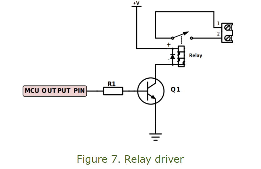
The output from the ACMP is connected to the input of the relay driver, which is implemented as shown in Figure . The relay used in this design needs 100mA for its coil. In order to achieve that, a simple BJT transistor relay driver circuit was used.
In order to display the measured temperature and desired temperature, two 7-segment LED displays with common anodes were used.
Due to the pin number limitation of the SLG46620V, it is necessary to implement a display driver that can multiplex outputs between the two digits fast enough so that human eye cannot notice the switching. The common anode is used to enable/disable each digit, so that when one digit is displayed the anode for that digit is set HIGH, while the other digit's common anode is LOW. Figure 8 shows the common anode 7-segment display schematics.
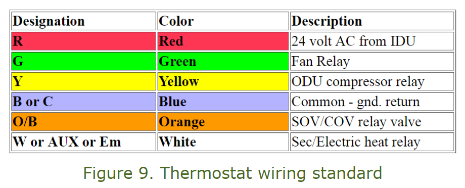
Figure 9 shows the standardized wiring colors for a thermostat. This design is using the R, Y, B and W wire connection points.
2. GreenPAK Implementation
This thermostat design is implemented using a GreenPAK IC, LED display, and temperature sensor. Additionally, it has a pushbutton for mode select (heating or cooling), a pushbutton for displaying set temperature, and two relays (one for heater control and one for compresor control).
Figure 10 depicts the thermostat logic implementation inside the GreenPAK. The initial polarity of DFF8 is HIGH which means only Relay 1 is enabled (PIN18), and Relay 2 is disabled (PIN19).
Switching to cooling mode is done by changing state of DFF8. The CLK input to DFF8 is connected to PIN2 which is connected to an external pushbuton. The output of ACMP2 is connected to Pipe Delay1, which is used to ensure that state of the relays cannot be cycled back on for approximately 1 minute.
The Pipe Delay1 component is a customizable shift register which allows the user to select how long they want the shift register to be, from 1 to 16 DFFs. CNT7 is used as the CLK source for Pipe Delay1. Using the configuration shown in Figure 11, the Pipe Delay delays the output of ACMP2 by 38 seconds. CNT7/DLY7 works in counter mode with output period of 2.37 seconds.
delay time = tp * OUT1 PD num = 38 s
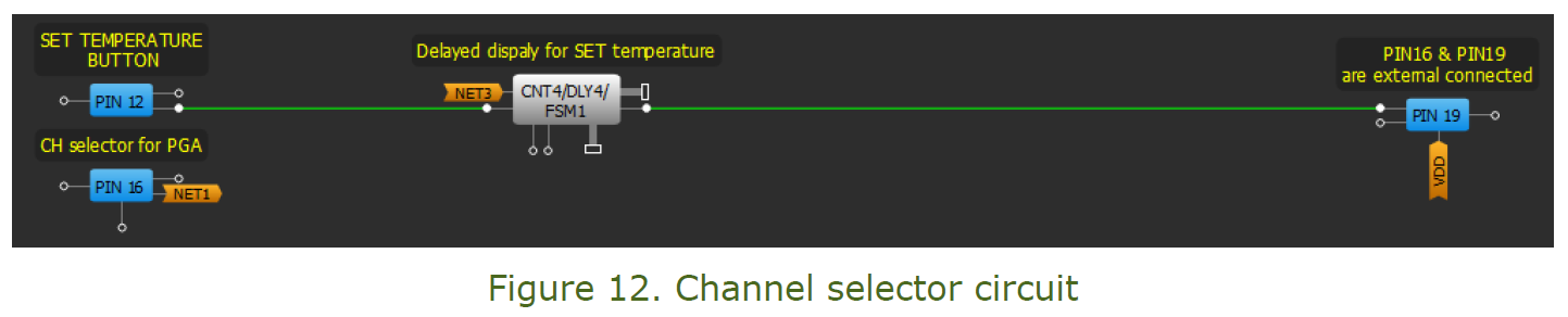
In order to be able to display both desired and measured temperature, the channel selector for the PGA block was used. The PGA has two input channels, IN+CH#1 and IN+CH#2. IN+CH#1 is connected to the temperature sensor, and IN+CH#2 is connected to the potentiometer. Pin12 is connected to the input of CNT4/DLY4.
The counter's output is connected to Pin19, which is also connected to Pin16 externally. When the pushbutton is released, CNT4/DLY4 will delay its falling edge by 2.36 seconds. This will allow the user to see the set temperate, as the default temperature shown on the display is the measured temperature. This channel selector circuit is depicted in Figure 12.
The output from the Programmable Gain Amplifier (PGA) is the input to the ADC block. The 8-bit output of the ADC block is passed to the FSM0 block, which will generate pulses based on the value of the 8-bit ADC data.
The CLK for FSM0 is CNT1/DLY1, which generates pulses with a 1.2ms period. When FSM0 reaches the set value provided by the ADC, it will generate a pulse and start counting again from zero. The SLG46620V has an 8-bit ADC, so the ADC data will range from 0-255. For example, if the ADC data is 128, we can calculate the period of pulses generated by FSM0 as:
Tp = ADC data * 1.2 ms = 153.6 ms
The ADC has 1.2V/256 samples resolution, which is aproximately 0.004V/sample. Therefore if the ADC data is 128, it indicates that the voltage is equal to 0.512mV. Using the FSM and ADC, we are able to convert an analog voltage to time.
Figure 14 depicts the architecture of the implemented display driver. This design is based on a modified architecture of the LED display driver explained in AN-1075 - GreenPAK Voltmeter with 2 digit LED display.
This display driver will map changes of input voltage in from the ADC from 0 – 1 V in range of digital numbers from 0 to 99 and show them on two 7-segment displays. In order to explain the display design, lets look at an example where the input voltage in the ADC is 500mV:
- Vin = 500mV
- n=8, 8-bit ADC
- ADC reference = 1V
- ADC step = 3.9 mV/sample
- ADC value that will be passed to FSM0 = 500/3.9 = 128
The input clock for FSM0 has a 1.2ms period, so FSM0 will generate a pulse after (128 * 1.2) ms = 153.6ms. When FSM0 outputs a pulse, the decimal counters connected to it will reset and begin counting again, while the latches forward data to the decoder. There are two decimal counters (DC's). DC1 is used to count least significant digits, and DC2 is used to count most significant digits. DC1 will reset itself when it counts to 10. The CLK used for DC1 is CNT0/DLY0 with period 3.072ms. A CLK edge for DC2 is generated when DC1 reaches 10. When FSM0 generates a pulse that resets the DCs, they will start counting, and at the next reset DC1 will generate 153.6ms/3.072ms = 50 pulses.
After 50 pulses, DC1 will have 0 stored and DC2 will have 50/10=5. When FSM0 generates a second pulse after an additional 153.6ms, the DCs will reset and latches connected to each bit of both DCs will pass data to the decoder circuit. The implemented decoder can only handle one digit at a time, which means that the least and most significant digits must be passed to it one at a time. Each display digit has a control pin which can enable/disable it since the data pins are connected in parallel. Data passed to the decoder is multiplexed using DFF9 and OSC components. Digits will be displayed at a frequency of 10.415kHz. Control of both digits is synchronized, so that when the first digit is enabled, latches connected to DC1 will pass the data to the decoder circuit shown in Figure 16.
The thermostat will show data in the range 0°C do 37°C. Due to this limitation, DC2 does not need to count all the way to 9, and can be cut off at 3, which is a modification we made to AN-1075.
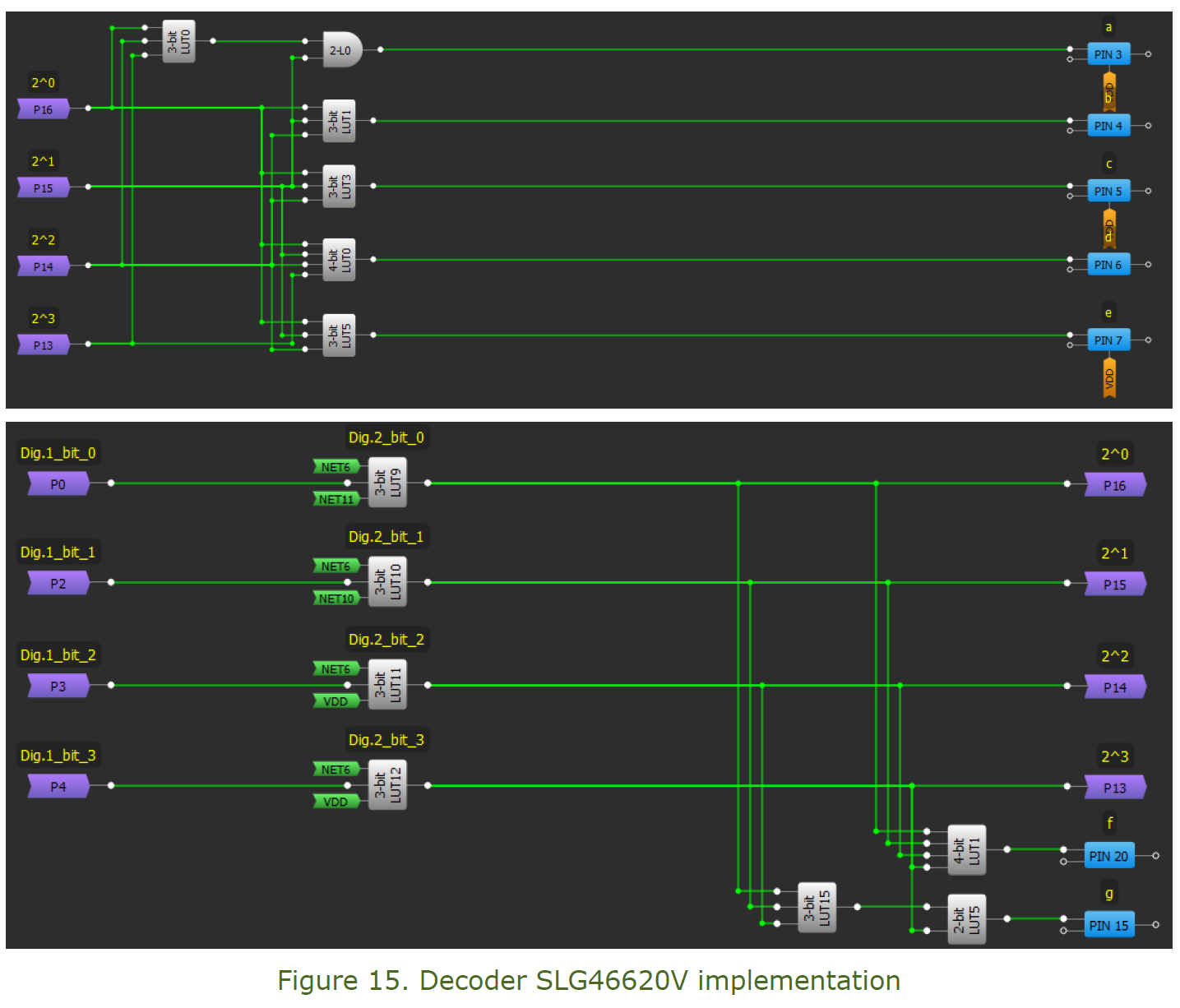
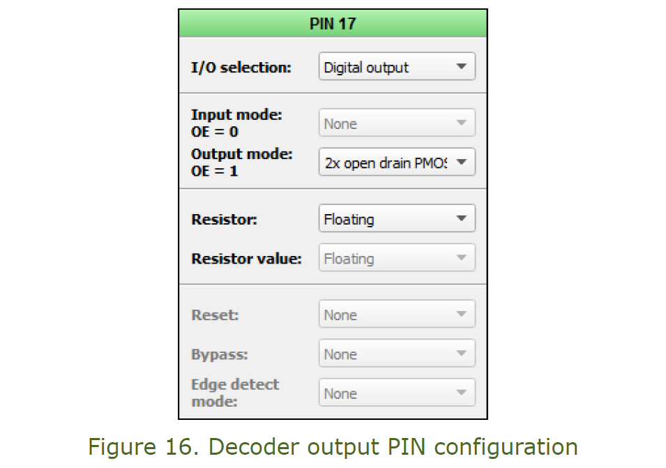
Figure 16 shows the configuration for the output PINs from the decoder, which are used as LED drivers. Each output is configured as a 2x open drain PMOS.
The display logic is implemented to map the 0-1V voltage range to the 0-99 digit range, but the thermostat's working range is only has 0°C to 37°C. The temperature sensor used in this design will output 500mV at 0°C, which corresponds to the number 50 counted by DC1 and DC2.
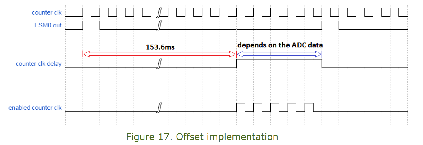
This means that an offset is needed in order to display the correct temperature.
As another example, when the room temperature is 25°C, the sensor output will be 750mV which corresponds to digits 75. In order to show the correct temperature, a 50 digit offset is implemented. This is done by delaying the DC1 reset for 50 pulses after FSM0 generates a pulse. 50 pulses is equivalent to 153.6ms. This is depicted in Figure 17 and Figure 18.
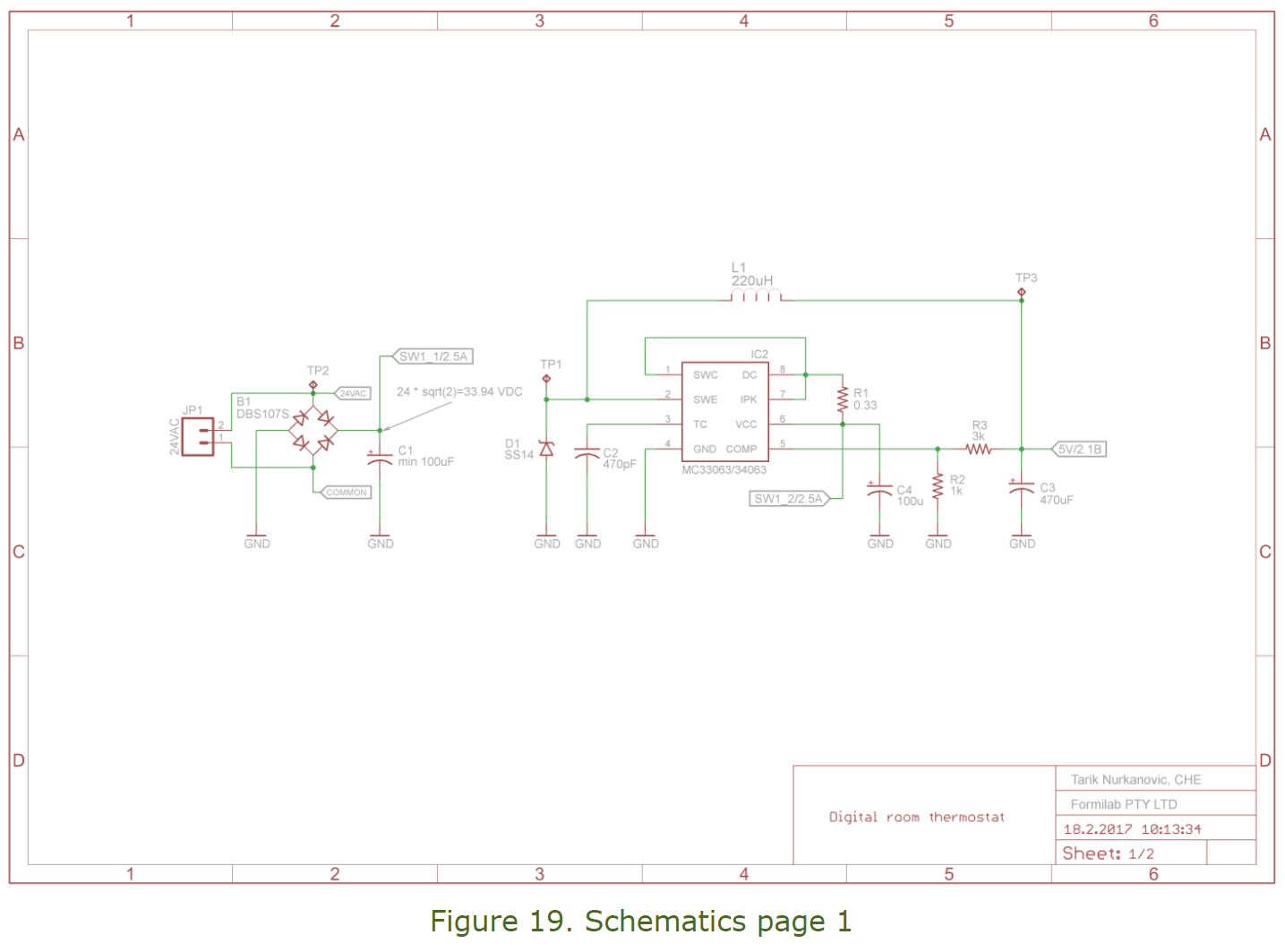
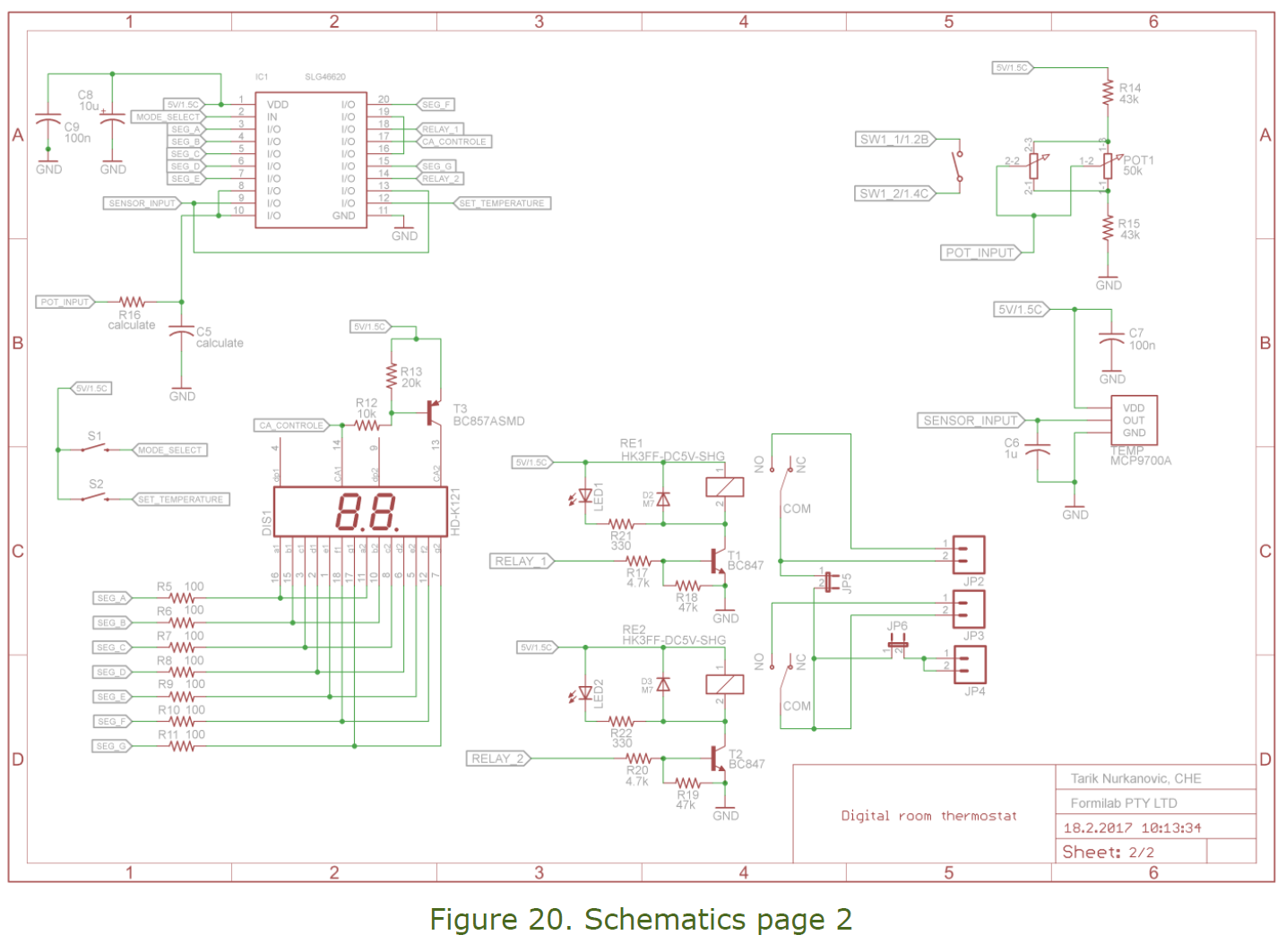
Figures 19 and 20 show the complete electrical schematic for the thermostat design described in this project.
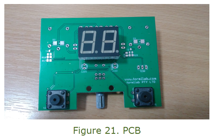
Figure 21 shows the PCB photo of the complete thermostat design described in this project.
Conclusion
The thermostat design we implemented in this project covers the core functionalities of a room thermostat. Additional features like power glitch handling can be solved using an external battery and power regulation circuitry that will detect power failure and supply the GreenPAK from an auxiliary battery in order to save flip flops states. This project shows that GreenPAK ICs can implement a room thermostat thanks to its flexibility and configurability.