This project provides details of RPWM signal generation for driving three-phase inverters using the SLG46620.
Below we described steps needed to understand how the solution has been programmed to create the RPWM three-phase inverter. However, if you just want to get the result of programming, download GreenPAK™ Designer software to view the already completed GreenPAK Design File. Plug the GreenPAK Development Kit to your computer and hit the program to design the device.
In power electronics, several Pulse Width Modulation (PWM) schemes have been successfully employed depending on the particular application. Most of the conventional PWM schemes, being deterministic in nature, produce a predetermined harmonic content. This can create a number of issues in real-world applications like the production of acoustic noise, radio interference, and mechanical vibration. In applications where interference with the environment and other equipment need to be mitigated, for example in industrial motor drives, traction drives, electric vehicles, the conventional PWM schemes inherently do not perform efficiently and additional equipment like electromagnetic interference (EMI) filters need to be added [Bhattacharya, Subhadeep, et al. "A discrete random PWM technique for acoustic noise reduction in electric traction drives." Energy Conversion Congress and Exposition (ECCE), 2015 IEEE. IEEE, 2015]. One available option to cope with issues resulting in these applications is to increase the switching frequency of the conventional PWM schemes i.e.>18kHz [Capitaneanu, Stefan Laurentiu, et al. "On the acoustic noise radiated by PWM AC motor drives." Automatika 44.3-4 (2003): 137-145]. However, this causes the switching losses to increase significantly. In such applications random pulse width modulation (RPWM) has been found to be effective to mitigate the cited issues without the need of considerably increasing the switching frequency.
In RPWM the width of each switching pulse varies stochastically. This causes the harmonics cluster to spread over a large range thus reducing the size of separate filters or entirely avoiding the use of filters in certain applications. RPWM technique has successfully been utilized in many power electronics applications e.g. in industrial motor control drives where the acoustic noise needs to be checked.
Usually, high-frequency PWM and RPWM signals for commercial sophisticated systems are implemented using Digital Signal Processors (DSP) and Field Programmable Gate Arrays (FPGA). However, these devices are more generic, powerful, and flexible which makes them quite expensive. Similar precision and high-frequency timing requirements needed for RPWM generation can be met with a low-cost Dialog GreenPAK IC. Many suitable RPWM schemes, especially for open-loop applications, can be implemented using Dialog ICs. Thus, the explicit programming or coding of embedded DSPs, MCUs or FPGAs is replaced by a simple interface provided in the GreenPAK designer. In addition, the size of the overall control circuit is considerably reduced.
There are several ways of producing the RPWM for three-phase inverter applications. In this project, a suitable RPWM technique is presented that can be implemented using the available GreenPAK IC's resources. The RPWM technique is implemented using the dual matrix SLG46620 IC. Appropriate theoretical proposals and experimental results are also presented including the output voltage waveforms and their harmonic content that would justify the proposed strategy.
Proposed RPWM Scheme
The block diagram of the RPWM scheme driving a three-phase inverter is shown in Figure 1.
Two saw-tooth signals, labeled as p2 and p3 (with values ranging: 0-1), 180 ˚C phase apart, are compared with a constant value p1 (with value ranging: 0-1) to give different type of pulses labeled as p5 and p6. The waveforms of these pulses (p5 and p6) are shown in Figure 2 and Figure 3. A binary pseudo-random number generator (labeled as p4) with the waveform shown in Figure 4 is employed to randomly select a pulse out of the signals p5 and p6 using the logical operators as shown in the above block diagram. This generates a train of pulses p10, which is shown in Figure 5. The signal p10 is passed through AND gates along with 10ms long pulses generated by pulse generators 1 through 6 and tagged as p11, p12, p13, p14, p15, and p16. Note that, the pulse generator output pulses have 60 ˚C phase difference relative to each other for a full 180 ˚C conduction mode. Finally, after AND operations, the signals p17, p18, p19, p20, p21, and p22 become the gate driving signals for the power switches employed in the power stage of the three-phase inverter.
The switches (usually MOSFETs or IGBTs) are switched on and off according to the applied gate signals to obtain the three phase balanced voltage waveforms at the output of the inverter.
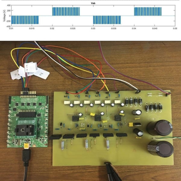
A simulation is carried out in Matlab/Simulink environment for a 50 Hz (fundamental) RPWM three-phase inverter system and the phase-phase output waveforms are shown in Figure 3. Effectively, the output voltage waveforms are modulated by the stochastic signal p10 and shifted from one another by 120 ˚C.
Selection of Reference Value
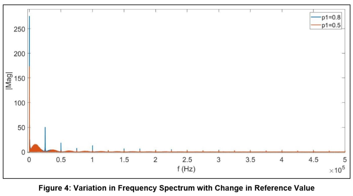
The reference signal p1 provides a way to control the spectral content of inverter outputs for a particular application according to the subjective acoustic response. Variation of the reference from 1 to 0.5 flattens out the spectral content mitigating the spikes at the multiples of the switching frequency. However, it also reduces the magnitude of the fundamental component of the signal. Figure 4 illustrates how the spectral content of the output phase-phase voltage changes by decreasing the reference value from p1=0.8 to p1=0.5, for Vdc = 312 V and carrier frequency =12.5 kHz.
Decreasing the value further from 0.5 is not recommended as it starts to increase the spikes at the multiples of the switching frequency and the fundamental component is also reduced.
GreenPAK Design
Figure 5 shows how the selected Dialog GreenPAK IC SLG46620 fits into the entire scheme. The basic operation of the IC is to generate the random pwm modulated signals that are applied at the gate terminals of the switching devices used in the inverter power stage.
The fundamental frequency of the inverter output voltage is chosen to be 50 Hz. SLG46220 is chosen because it provides sufficient resources to carry out the intended design. The Matrix 0 and 1 designs are shown in Figure 6 and Figure 7 respectively. In Matrix 0 a pseudo-random signal (PBRS) P0 is produced by connecting DFFs in a concatenated fashion and using a XOR gate in a feedback loop as shown in Figure 6. The DFFs are driven by a 12.5 kHz clock signal from OUT0 of the oscillator block.
For the saw-tooth carrier signal generation, the use of FSM blocks is proposed. Both FSM0 and FSM1, configured in set mode with UP=0, are fed by counters CNT1/DLY1 and CNT3/DLY3 respectively that create pulses having a frequency of 1.6875 MHz. The counter value in both FSMs is set as 134 (output period 80 us) to achieve the desired 12.5 kHz discrete saw-tooth signal. To achieve 180 °C phase shift between the both saw-tooth signals FSM0 is enabled 40 us after FSM1 using a pipe delay fed by CNT9/DLY9.
The two saw-tooth carrier signals are fed to DCMP0 and DCMP1, via the Q byte output ports of FSM0 and FSM1, for comparison with a constant reference signal (configured inside the registers DCMP0 and DCMP1) as shown in Figure 7. Since the counter runs up-to a value of 134 the reference value is given with respect to 134 e.g. 67 would be equivalent to the value of 0.5 (67/134). The outputs of the two DCMPs (p5 and p6) are further passed through to two AND gates along with the output signal from the LFSR (p4) and its inverted value (p7). An OR gate is fed with the output of these AND gates to randomly obtain one of the two outputs of the DCMPs. The output of the OR gate (p10) is further used to modulate the driving signals of the inverter.
The counter CNT0/DLY0 is configured to produce pulses with a 10 ms period in order to have output voltages of 50 Hz frequency (fundamental). These pulses are fed to a DFF configured in an inverting mode, with the output fed back to the input, to produce a 50 Hz square wave pulse train. To ensure that the output pulses labelled as p11 through p16 are 60 °C phase apart, the use of a pipe delay block is proposed. The counters CNT5/DLY5, CNT6/DLY6 and CNT7/DLY7 are cascaded to provide pulses with a period of 3.33 ms. These pulses are fed to a pipe delay through a not gate since the pipe delay creates delay by counting the number of input rising edges whereas the counters, get reset to 0 with the reset input, create coinciding falling edges with a period of 3.33 ms. Out 0 and 1 of the pipe delay provide 3.33 ms and 6.66 ms time delays respectively to the input pulse. The three signals i.e. input and the two delayed outputs of the pipe delay are further inverted to provide a total number of 6 pulses (p11-p16) that are 60° phase-shifted to each other. These 50 Hz, 60 ˚C phase-shifted pulses are further passed to AND gates along with the random pulse train (p10) to provide the final driving signals for the 3 phase inverter.
Experimental Results
A hardware prototype depicted in Figure 8 was developed to experimentally validate the proposed RPWM scheme. To ensure that both switches in the same leg do not turn on at the same time a dead band was produced in hardware.
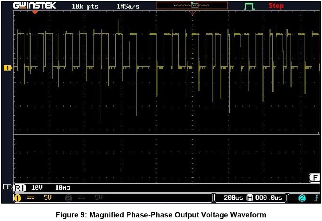
Figure 9 shows the magnified waveform of the output phase-phase voltage. It is evident that the waveform is randomly modulated as desired.
In Figure 10 the output phase-phase voltage signals Vab (in yellow color) and Vac (in blue color) are shown. Moreover, the FFT plot of Vab (in red color) for reference value ≈ 0.8 (107/134) is also depicted. Though the spread in the frequency spectrum is evident, a spike at twice the switching frequency i.e. 25 kHz is observed as the theory suggests.
Figure 11 depicts the output phase-phase voltage signals Vab (in yellow color) and Vac (in blue color) as well as the FFT plot of Vab (in red color) for reference value = 0.5 (67/134). It can be seen the spectrum gets flatter and significant spread is also achieved.
Conclusions
RPWM signals for three-phase inverters can be generated using different techniques and usually expensive DSPs and FPGAs are used in industrial applications to achieve the desired results. In this project, a suitable RPWM generation technique for three-phase inverter applications using a low-cost Dialog SLG46620 GreenPAK IC has been outlined. Through appropriate simulations and experimental results, it has been established that the proposed technique is functional and SLG46620 IC provides sufficient resources to carry out the intended results.