Try your hand at this do-it-yourself resistor-transistor logic gate.
We all love our modern devices ranging from smartphones to smart cars and all of it is made possible thanks to the transistor! The technology we use has only been around for a few decades, so how did engineers in the past create complex digital circuits? This also brings up the question “how did NASA build a computer that was small enough to fit on the Apollo modules?” The answer lies in RTL which stands for resistor-transistor logic which for a while was one of the most popular logic families.
Logic Gate Schematics
While there are many logic gates that exist, the three gates that will be shown here will be the fundamental gates (those that use the least number of parts and can be used to make every other logic gate). These gates are the NOT gate, NAND gate, and the NOR gate.
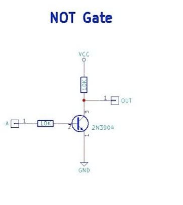
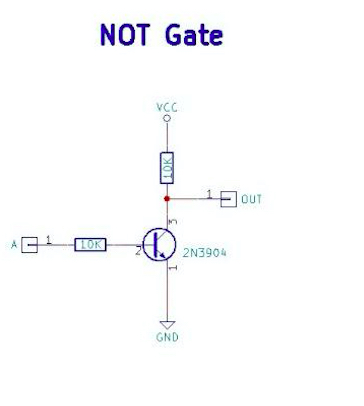
The NOT gate consists of a single NPN transistor, a collector resistor, and a base resistor. When the input is connected to 0V, the transistor is switched off and does not conduct any electricity. This means that the voltage at the collector will be equal to the supply (if the output is unconnected). If the input is then connected to VCC, the transistor fully saturates (i.e. switches on), and effectively connects the output to ground (0V). Hence, the operation of the NOT gate is performed.
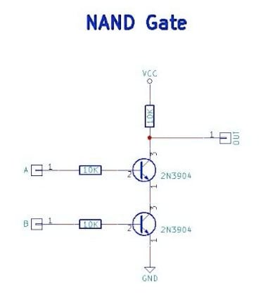
The NAND gate consists of two NPN transistors in series, each having a base resistor (for current limiting) and a single collector resistor. When both inputs are off (0V), both transistors are turned off and therefore the output is connected to VCC through the collector resistor. If either input is turned on (but not both), then the transistor that is turned on will conduct, but the transistor that is turned off will not conduct current. Therefore, the output remains connected to VCC through the collector resistor. If, however, both inputs are connected to VCC, then both transistors are turned on. This means that the output is connected to 0V through both transistors and therefore the output is off, thus realizing the function of the NAND gate.
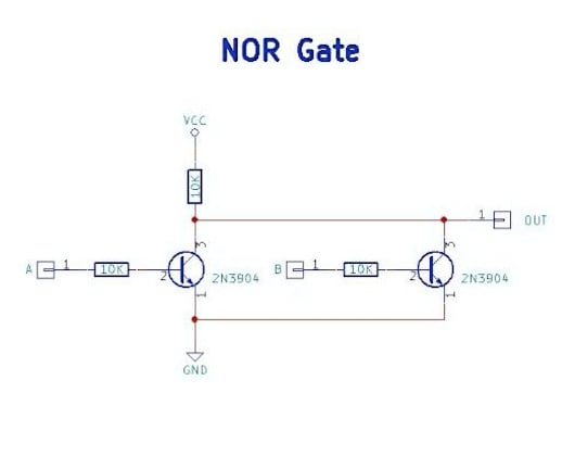
The NOR gate also consists of two NPN transistors which are arranged in parallel. If neither input is turned on then none of the transistors are turned on and therefore the output is connected to VCC via collector resistor. If either input is turned on, then the corresponding transistor turns on and thus connects the output to ground via that transistor. Even if both transistors are on, the result is still the same and the output remains off, thus realizing the NOR function.
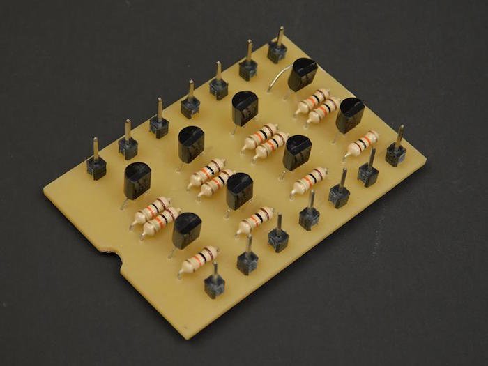
Constructing Your RTL Logic Gates
Building RTL logic can be built using any construction technique. However, when building RTL systems, you need to consider the size of the circuit that you wish to construct. For example, building a single gate can easily be done on breadboard or stripboard but if you plan to build a computer then you need to consider methods for saving space and time. So, the RTL NAND gates demonstrated here are built on a PCB that holds four NAND gates in the same pinout as many popular 4000 series chips. This means that this larger package can be mounted and then wired to other logic clusters which makes wiring much easier.
Four NAND gates on a single PCB
This four-gate package could be made much smaller if made on a double-sided PCB. If surface mount parts are used, then the size could be reduced even further and make large scale projects easier. I hope you learned a little about logic gates. If you've made your own logic gates, please share them in the comments!