In this article, I’ll explain those diagrams and teach you how to read and interpret them easily!
In a previous article, I discussed important considerations to make when choosing the right parts for your digital designs. One consideration mentioned is the importance of considering the timing restrictions of the ICs you may use.
You can find timing restrictions in the datasheet of a component in the form of a timing diagram.
Asynchronous and Synchronous Devices
In synchronous digital circuits, the state (usually of some memory blocks) is only changed with a synchronous clock. In an ideal circuit, there would be no delay between the clock signal and the effect that takes place in the device. Unfortunately, this ideal isn’t possible in the real world.
An asynchronous circuit, on the other hand, is a self-timed circuit that isn’t governed by an external clock. Instead of finishing after a certain number of clock pulses, it signalizes when it’s done with whatever task it was carrying out.
However, timing diagrams are not limited to one kind. Usually, they come with every integrated circuit, no matter how complicated or simple they are. For example, the 7400 NAND gate comes
Reading and Interpreting Timing Diagrams
Timing diagrams can be intimidating when you first look at them, especially for unexperienced makers. Furthermore, almost all of them are a bit different, because every manufacturer and author of the datasheets creates them a bit differently, just like everyone has a unique handwriting.
However, timing diagrams are made to help you to understand the functionality of a device, so they all want to convey the same message.
Let’s look at a more complicated timing diagram, taken from TI’s datasheet for their various synchronous 4-bit counters.
The designer was kind enough to include a few notes (at the bottom of the diagram) that describe what the chart supposed to represent. This makes it easier for us to understand what’s going on.
Let’s look at the first operation, which is the asynchronous clear. We can see that the outputs all go low as soon as the CLR input goes low. The synchronous clear, however, only happens when the CLK signal goes high the next time:
In general, you shouldn’t look at these diagrams isolated from the rest of the document. If you look for the general description of the device’s function, you’ll find the following information:
“The clear function for the 160, 161, (...) is asynchronous and a low level at the clear input sets all four (...) outputs low regardless of the level of the clock. (...) The (...) 163 is synchronous and a low level at the clear input sets all four (...) outputs low after the next clock pulse (...).”
As you can see, the timing diagram is an addition to the textual description to make it easier to visualize the operation of the device.
Knowing this, let’s continue by looking at the counting process. In this example, the counter is preset to twelve:
As you can see, the input data was present long before the load operation was triggered. The load input went low with the last clock pulse. The data, however, is only latched with the next pulse, as indicated by the purple line.
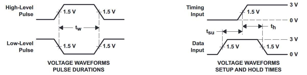
You’ll also usually find a table with timing constraints that describe how long certain signals have to be stable to guarantee flawless operation of the device.
Thus far, ENP and ENT were both low. For the device to start counting, both have to be high. So, for the next operation, both go high at least 20ns before the next clock pulse occurs. Then the counting begins and continues until either ENP or ENT gets low again.
When either of them is low, the device's internal output latch retains the current count.
Use Text and Diagrams Together!
As stated above, every company has its own style when it comes to timing diagrams. Therefore, you always have to look at these diagrams in combination with the accompanying text. Sometimes, it’s difficult to understand the descriptions, especially if they contain a lot of different numbers. However, things are usually easy to understand once they are visualized in a diagram.
Don’t be intimidated by complicated looking diagrams. They are often easier to understand than the text that describes them. Make sure to look at all the inputs and precisely observe how the outputs change. Furthermore, you should search for a table that describes the timing constraints of the device. As stated above, state changes are not instant. Input signals usually have to be stable for a certain time, so that the circuit can reliably detect them.