Learn all about Logic Level Shifters and where they are best used depending on your components!
A logic level shifter, or a voltage level translator, is used to translate signals from one logic level to another. Nowadays, most of the system runs on 3.3V or 5V. Logic level is simply a HIGH and LOW level of voltage for a certain board or IC. Knowing this, a logic level shifter is necessary to create a path between processors, sensors, or boards of different voltage levels.
Let's look at an example. When you want to interface an ESP8266 module that runs on 3.3V with an Arduino UNO which is a 5V board, you need a level shifter to translate the 5V signals to 3.3V and vice versa. Otherwise, you may damage the ESP's silicon.
Common Logic Levels and When They Are Used
Currently, the three most common logic levels are 1.8V, 3.3V, and 5V. Why these standards? The simple reason for this is these are the voltages required to activate the transistor logic of a board or IC.
For a single transistor logic like a NOT gate, we need to apply a voltage greater than 0.7V at the base of that transistor to activate it. So for a single transistor logic, a voltage greater than 0.7V is logic1 and anything less than that is logic0.
Now when a transistor is used to drive another transistor, we need to double the voltage from that of a single transistor. So here, the threshold voltage will be 1.4V. Another example is DTL (diode transistor logic). A diode has a forward voltage drop of 0.7V and so we need 1.4V to activate the circuit. A good amount of margin is safe and so 1.8V is kept as a standard for these circuits.
For multiple transistors to do a task, a higher voltage level of 3V or 5V is required. So, processors or boards have different voltage levels and all these boards, processors or sensors need to co-exist for various applications and that is done by forming logic level shifter bridge for translation.
Almost all of the new families of boards and sensors work at a 3.3V logic level. If they need to be interfaced with a 5V board like an Arduino UNO, voltage translation is needed. However, there are certain cases where we don’t need any translation circuits for interfacing two boards of different voltage levels.
We all know from basic electronics that most of the time, a voltage level greater than 2V is logic1 for most boards and a voltage level of less than 0.8V is logic0. So by this, we can easily apply 3.3V signals to a 5V processor/board without an additional circuit. But, of course, it is necessary to check the datasheet of the IC in use for threshold voltage level.
For reverse conditions when we want to apply 5V signals to a 3.3V board, some boards consist of clamping diodes to protect the silicon from high voltage. In this case, a big resistor in series will do the trick. But it all depends on the board you use. Now let’s look at some translating circuits.
Design a 5V to 3.3V Translation Circuit
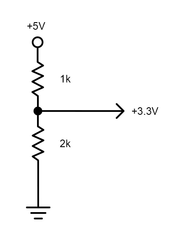
To translate 5V signals to 3.3V signals, the simplest way is to make a voltage divider. A voltage divider consisting of a 1k and 2k resistor can perform this task. The output voltage of a voltage divider can be calculated by the following equation:
Rx will be the resistor across which we measure output. In this particular case, it would be a 2k resistor. For example, when you need to interface a 3.3V SPI device with a 5V board, you just need to connect the MOSI, CLK, and CS pins with a voltage divider and leave the MISO pin unconnected.
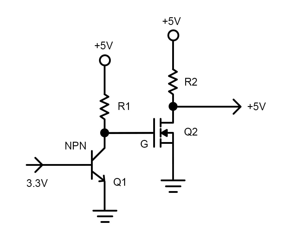
Designing a 3.3V to 5V Translation Circuit
For invert translation, we need a two-transistor logic.
We arrange two inverting configurations of a transistor in series to get a non-inverting +5V output. When we apply 3.3V to the first transistor, it will be saturated and will provide the inverting signal to the second transistor, which will again invert the level and provide +5V signal at the output. Also, we need to consider the voltage drop across resistor R2 and understand that using an N-channel MOSFET instead of an NPN transistor at Q2 will provide a low dropout output very near to +5V.
The Logic Level Shifter for Multiple I/O Lines
In the case of multiple I/O lines, it is better to use a Schmitt trigger IC. The hex non-inverting Schmitt trigger IC 74HC4050 is a good option for this task. A Schmitt trigger is actually a comparator circuit that converts the analog input to digital signals; in short, it fastens the signals.
However I2C devices can't be interfaced using these translating techniques, so we need a bidirectional logic level shifter for this task. The IC 74LCX245, a low voltage bidirectional logic level shifter, can be used for this. You can apply a 3.3V voltage level with the help of LM317 IC to the translator IC.
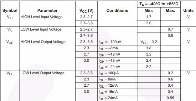
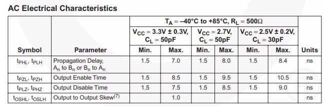
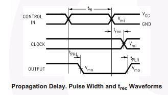
It’s very much worth noting the voltage threshold levels and delays associated with these ICs. Datasheets of both ICs provide an easy to use table for delays and voltage levels. I recommend going through them to check if these ICs are suitable for your applications.
Threshold voltages data for IC 74LCX245
Propagation delay waveform
Source: IC74LCX245 datasheet
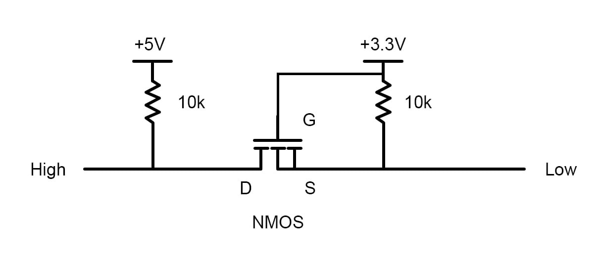
Bidirectional Logic Level Shifter Circuit
A simple bidirectional logic level shifter is built around a single transistor and, as the switching speed is not an issue, is a very handy and convenient circuit.
When HIGH (pin) is logic1 (i.e., 5V at that pin), the drain and source of the MOSFET are pulled high. Gate voltage will be lower than the source voltage in this case and so MOSFET is in the cut-off region (i.e., inactive). Thus, the LOW pin is pulled at 3.3V as no current flows through the gate. When HIGH is logic0, the gate voltage is greater than the source voltage which will pull the LOW pin output down.
Similarly, when LOW is logic1, then Vgs (gate-source voltage) will be 0 and so the transistor will be inactive pulling the HIGH pin to +5V. When LOW is logic0, the gate voltage is again higher than the source voltage and the HIGH pin is pulled down.
In this article, we have discussed logic level shifters, looking at why and when they are needed. We have seen some translation circuits and some ICs for multiple line translations.