Learn how to use GPIO on STM8 microcontrollers, as well as which datasheets you need for a successful project.
In the last article, Getting Started with STM8 Microcontrollers, we looked at how to get started with STM8 microcontrollers, including IDE installation and getting a free license for the COSMIC c compiler. In this article, we will learn how to use GPIO on STM8 devices as well as which datasheets you need to use.
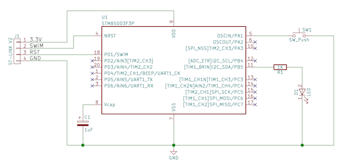
Schematic
A Generic Design
When using PIC and AVR devices you typically need to get the datasheet for that specific device and learn how to use the peripherals. Sometimes, a peripheral on one PIC may not be the same as on another PIC, so code cannot simply be copied and pasted from one PIC to another. However, the STM8 is completely different, as all STM8 devices use a generic layout instead of having unique configurations. This means that code designed for one STM8 can be directly copied and pasted to a different controller and it will still work (assuming that the new device has the needed peripherals).
One classic example is the UART peripheral. The STM8 devices can have up to three UART ports (1, 2, and 3) and UART1 on one STM8 device will be identical to UART1 on another STM8 device. However, the datasheets for individual STM8 devices do not contain much information on how to use the peripherals, so when working with any STM8 device you will need to use datasheets; the device-specific datasheet that includes pinouts, and another datasheet that contains the device-family specifics.
For our STM8 projects, we will be utilizing information from these two datasheets:
If you want to know where the pins are on a device, use the Device Datasheet and if you want to know about how to use a peripheral, use the Family Device Overview sheet.
GPIO
While the dev board allows us to program the STM8 microcontroller and play around with the CPU features, it's kind of pointless unless we can connect our micro to other devices and external circuits. To be able to do such tasks, general purpose input output, or GPIO, are used. GPIO are pins on the device that can be electrically connected to external circuits to control them or read information from them. While analog data can be read, this tutorial will only be concerned with digital values (those that are either on or off).
When it comes to GPIO, there are four main registers:
- DDR – Data Direction Register
- ODR – Output Data Register
- IDR – Input Data Register
- CR1 and CR2 – Control registers
Accessing Registers and Bits
Accessing GPIO on the STM8 is somewhat similar to AVR, with the exception that the STM8S.h uses structures. For example, PORT B on the STM8S has its own structure called GPIOB, and inside that are all the registers that control it (such as DDR, ODR, IDR, etc.,). Accessing these registers can be done as shown below:
GPIOB→xxx where xxx is the register in question
Data Direction Register (DDR)
Just like PIC and AVR devices, the STM8 uses data direction registers to determine if pins are either inputs or outputs. These registers are 8 bit wide and directly correspond to the pins on the I/O port. For example, PORT B can have up to 8 pins and B0 corresponds to bit 0 in the Port B DDR register while B7 would correspond to bit 7 in the Port B DDR register.
To configure a pin as an input, the corresponding DDR bit needs to be cleared (0), and for an output, the bit needs to be set (1). So let's say, for example, we wanted to configure only B0 and B1 as inputs while keeping the rest as outputs. We could do the following:
GPIOB→DDR = 0xFC;
or
GPIOB→DDR = 0b11111100;
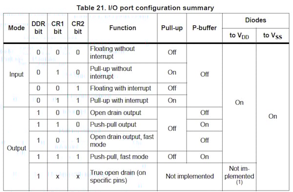
Control Registers CR1 and CR2
CR1 and CR2 are control registers that can be configured to provide different I/O features. For example, they can be configured to allow for interrupt generation on individual pins and can be used to create output drivers with push/pull capabilities. Just like the other registers, each bit in the CR1 and CR2 registers corresponds to a specific pin. So, for example, bit 0 in CR1 and CR2 is used for pin 0 of a port. The table below (extracted from the datasheet) demonstrates what the CR1 and CR2 registers can be used for.
Output Data Register (ODR)
The output data register is used for outputting digital values (1 and 0) onto a port. Either individual bits can be written to (using bit masks) or the entire register can be changed. Writing a 1 bit to a ODR bit will make the corresponding pin turn on, and writing a 0 will make the corresponding pin turn off. The first example below is used to turn all the pins on a port on, and the second example turns all the pins off.
GPIOB→ODR = 0xFF; or GPIOB→ODR = 0b11111111; // Turn on all pins
GPIOB→ODR = 0x00; or GPIOB→ODR = 0b00000000; // Turn off all pins
Input Data Register (IDR)
The IDR register can be used to read the digital value found on the pins on a port. These values can be either on (1) or off (0) and bit 0 of the IDR register corresponds to pin 0 while bit 7 corresponds to pin 7.
pinRead = GPIOB→IDR;
Useful Bit Manipulation
Since I/O ports are made up of individual pins, it would be more helpful to access individuals bits as opposed to the entire register. However, individual bits are not available (similar to the AVR devices), so we need to use some bit manipulation. Since this has already been explained in the AVR series, we will only look at some macros that can be very helpful.
These are really useful macros that help to get rid of unreadable bit masking code:
#define setBit(reg, bit) (reg = reg | (1 << bit))
#define clearBit(reg, bit) (reg = reg & ~(1 << bit))
#define toggleBit(reg, bit) (reg = reg ^ (1 << bit))
Copy and paste this code at the top of your code, and you can then use them like functions instead of having to write bit manipulation code out. So let’s see some examples of how you would use these in your code!
setBit(GPIOB→DDR, 3); // Set bit 3 on port B to be an output
clearBit(GPIOA→ODR, 4); // Turn off output bit 4 on port a
toggleBit(GPIOC→ODR, 5); // Toggle bit 5 on port c
Reading pins, however, uses a simple bit of bit manipulation that involves using an AND to mask all the bits that we don’t want and then test to see if the result is 0 or not.
if( (GPIOB→IDR & 0b00000001) )
{
	// Code here executes IF bit 0 is on
}

if( !(GPIOB→IDR & 0b00000001) )
{
	// Code here executes IF bit 0 is off
}
Basic Configuration Example
In this example, we will configure pin A1 as an input and B5 as an output, and whenever the switch is pressed (which is connected to A1), the LED connected to B5 will toggle. Here we also take advantage of internal pull ups, so our button does not need a pull-up resistor to work (done by setting bits in CR1).
/* MAIN.C file
 *
 * Copyright (c) 2002-2005 STMicroelectronics
 */
#include "stm8s.h"

#define setBit(reg, bit) (reg = reg | (1 << bit))
#define clearBit(reg, bit) (reg = reg & ~(1 << bit))
#define toggleBit(reg, bit) (reg = reg ^ (1 << bit))

void simpleDelay(void);


main()
{
	GPIOA->DDR = 0x00;			// Make all pins on PORT A inputs
	GPIOA->CR1 = 0xFF;			// Ensure that internal pull up is on
	GPIOA->CR2 = 0x00;			// Ensure that interrupts are turned off

	GPIOB->DDR = 0xFF;

	while (1)
	{
		// Testing bit 1 (bit 0 would be 1)
		if( !(GPIOA->IDR & 0x02) )
		{
			toggleBit(GPIOB->ODR, 5);
			simpleDelay();
		}
	}
}


// Simple delay used for debouncing
void simpleDelay(void)
{
	unsigned int i, j;

	for(i = 0; i < 1000; i ++)
	{
		for(j=0; j < 10; j ++)
		{
		}
	}
}