You can purchase PCBs at low prices ($35 from DirtyPCBs), but even then, the price is high enough to be prohibitive for untested designs (remember, breadboard won’t work with these new devices). Of course, simulations can be done, schematics can be checked, and PCB designs looked at under a magnifying glass, but errors always find their way through. This leaves hobbyists with one alternative — to make their own PCBs.
The Two Main Options
PCB manufacture falls into one of two categories: milling or chemical processing. Each method has its pros and cons, but the method you choose depends on your capabilities and convenience. For example, I have a dedicated workshop, so either method is suitable. But someone who uses their kitchen to make PCBs may want to avoid a chemical route, as cross contamination can be potentially harmful to health. However, you must understand that choosing a production technique is like a marriage; you will need to commit and be faithful, or you may struggle to produce quality PCBs, since both methods require a level of experience and skill that you will attain as you make more and more PCBs.
Option 1: CNC Machining
Making PCBs using a CNC involves a small cutter that removes the excess copper from the PCB substrate. The size of traces and features you can make depends on several factors, including...
- Cutter width
- Machine accuracy
- Copper thickness
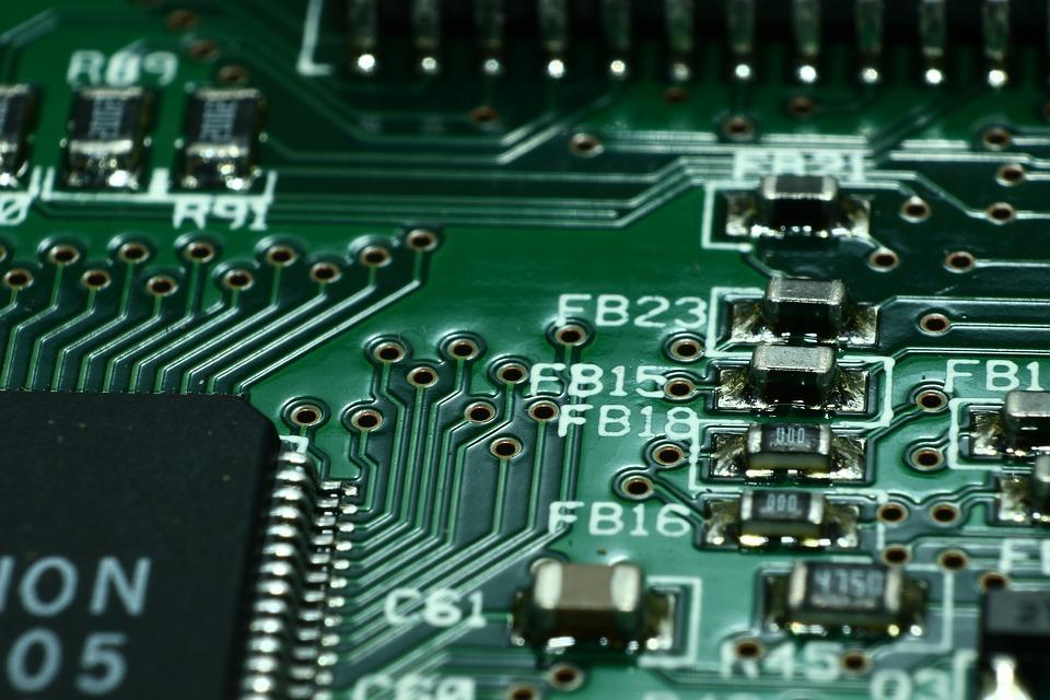
While features as small as 0.1mm are possible, the average CNC user can expect a trace width of 0.3mm with a clearance of 0.3mm. Making PCBs using a CNC has advantages over most other processes; most of the process is automated, and it allows for accurate drilling. It's also quicker to make a PCB with a CNC, despite the length of time needed to make the PCB itself, because fewer steps are needed to turn a piece of copper clad into the finished product. Another massive advantage of CNCs is that the machine can be made to do other jobs besides making PCBs, including woodworking and metalworking. Despite all its advantages, using a CNC to make PCBs comes with three main problems: cost, quality, and reruns. At their cheapest, CNCs are $700 pre-made (such as the CNC 3020). There are kits available that supply the motors and main parts, but not the framework; however, if such kits are built out of wood, the machine will have issues involving flex and squareness, which will result in poor-quality PCBs. But a pre-made CNC won't be perfect, either; adjustments will still need to be made in software to ensure accuracy. The next issue with CNC-made PCBs is their overall quality. Unless you use an expensive cutting bit, chances are the bit itself is not perfectly centered, and the result will be rough traces with signs of torn copper. But even if you have a perfect cutter, you will need to get the CNC bed perfectly flat if you don't use an auto-leveler. This brings us to the last issue — re-runs! Unless every step is carefully executed and care is taken, there may eventually be a problem that results in an unusable PCB.
Option 2: Chemical Processing
Chemical processing uses chemicals to make PCBs. The size of traces and features vary, depending on the specific process used. The two main process that are widely used are ...
- Toner transfer
- Photoboard/Dry film
Toner transfer uses glossy paper and a laser printout of the PCB layout to transfer the toner to the copper clad, which is then etched in an acid, such as ferric chloride. However, this process is not the most reliable, and often requires touch-up work to produce a functional board. To make matters worse, the quality of the transfer is dependent on the quality of the paper, the pressure applied with a clothes iron, the type of toner, the toner density, cleanses of the copper, and sometimes even the position of the planets! But the advantage of toner transfer is the simplicity of the equipment and the readily available laser printers and photo paper. For reliability, you can expect traces 12 mil wide with 14 mil clearance, but users have been able to go down as small as 8 mil. Photoboard and dry film are photosensitive and require a transparent printout of the PCB artwork. This artwork is then placed on top of the sensitive layer, compressed (to ensure artwork contact with the PCB substrate), and exposed to light. This method is incredibly reliable and repeatable, which makes it ideal for large runs. Unlike toner transfer, the artwork is reusable, as it is only used to block light. But unless multiple copies of the PCB are needed, each piece of artwork can be rather costly to produce (transparent film is expensive compared to photo paper). With the board exposed, it needs to be developed (typically with an alkali solution), cleaned, and etched. After etching, you use a stripping solution to remove the polymer that protects the copper layer from being etched. While PCBs made using a chemical process are high quality, they have some serious problems that must be addressed. The first issue is the number of chemical processes needed, which usually requires at least two chemical tanks. If you use dry film, you can expect to have at least four tanks! The second issue with PCB chemicals is that they are often dangerous (being an acid, alkali, or carcinogen). While small plastic containers can be used for making small PCBs, larger PCBs will need dedicated tanks. This results in a large area of chemicals coming in contact with the air, which can make them airborne. This is why you should dedicate a specific area to the tanks, and they should be inside a fume cupboard that has an extractor fan that blows outside. The last issue with chemically processed PCBs is the need for manual drilling (unless you own a CNC), which can be very difficult. If you use a CNC, you can make holes as small as 0.3mm, but if you drill manually, don’t expect holes smaller than 1mm.
The Verdict?
As irritating as this may be, the verdict is neither! Which is better for you entirely depends on your requirements. If you have small children and are worried about them being exposed to toxic chemicals, then go the CNC route. But if money is a concern, go for a chemical approach. If you're concerned about dust, go for the chemical process, since a CNC can make a lot of dust. But if you need to get PCBs out quickly, a CNC may be a better route. If you need to make many PCBs a week, then you must go chemical! But if you're someone like me who has a dedicated workshop, do both! Use a CNC to drill and cut out PCBs, and the chemical process to produce high-quality traces.
Related Articles