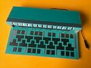
Hi, I’ve designed a really cool Stylophone-type keyboard with wrap-around keys for the second generation of my electronic ‘bagpipe’ project (discussed in a couple of audio threads here; see the image of my latest prototype below). The wrap-around keys work great! I’ve also got sharp/flat keys accessible both above and below the main keys.
Now I think I want to have a real circuit board fabricated. I’m a former graphic designer who hasn’t chased technology in a long time. I was thinking of designing the board in an old graphics program, saving the file(s) as PDF(s) and converting to Gerber files here: https://www.reaconverter.com/convert/pdf_to_gbr.html
Has anyone used that service? Has anyone gone from PDF to Gerber? Are there likely to be any glitches?
My main question though is about how to set up the graphics file. As a graphic designer, working in print, files always had to have crop marks and registration marks. Do I need to include anything like that in my graphics files for the PCB? Or is the edge of the document the edge of the board? And, I assume people do boards with rounded corners. Should I just draw an arc at each corner of the document? Otherwise, I’m assuming I need a separate page/graphic for top copper traces, bottom copper traces, drill holes, solder mask, and silkscreen. If I want holes in the corners for set-offs, they can be on the same page as the drill holes for components, right? Even though I‘d want a larger hole for the set-offs?
It all seems like a no-brainer to me, in terms of design for a 2-sided board. It’s super easy, in a vector-based graphics program, to layout everything in a master document, copy everything to a series of pages or new documents, and then eliminate everything except the solder masks on one page, everything except the drill holes on another page, etc.
I just need to know how to indicate the edges/corners of the board. Should I create a slightly larger document and just draw a rectangle with rounded corners for the border of the board?

