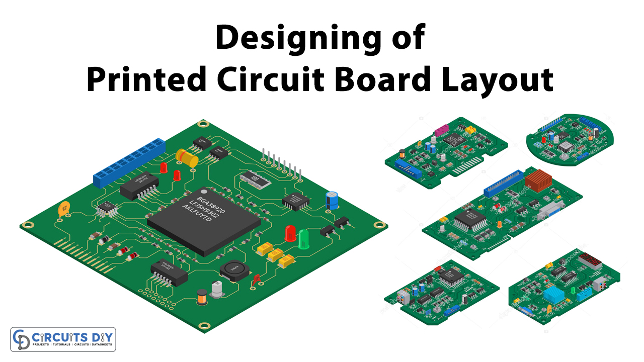
In this article, we are going to discuss Designing of Printed Circuit Board Layout
Introduction
In the electronics world, where Printed circuit board plays a crucial role, their manufacturing and fabrication also play an important part. But, before the manufacturing process, the process of designing is the biggest challenge. Here designing means, the designing of the circuit which is going to be manufactured on the printed circuit board. Very small circuits for the beginner cans directly be made on the board but usually, the designing is done on the various software created by engineers and available online. So, in this article, we’ll discuss the design tips for the printed circuit board layout. However, before starting, we are discussing different designing software.
Designing Software For PCB
Design software enables the designers to build a layout of PCB. It provides virtual board components and PCB libraries to build the design. The software also implements high-quality footprints of PCB and provides schematic tools to modify the electrical properties and other parameters of given board components. There are many designing software available like Altium designer, NI Multisim, Fusion 360, OrCAD, Autodesk eagle, dip trace, multi-board, cam 350, etc. Also, some of the software can be available free on the internet.
PCB Designing Process
The designing of the PCB requires several different steps. One can make an effective and reliable printed circuit board if designed intelligently. To make this easy for beginners, here we are going to describe some important design steps.
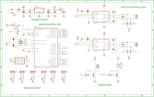
Build the Schematic
Schematic is actually the blueprint of your circuit. The building of the schematic includes the placement of the components and the connection of those components. As for the components, almost every software provides hundreds or thousands of libraries. Also, you can design your own design and use it as a component. This may give flexibility to your designs.
Routing
After the building of the schematic, this is time to route the circuit. Routing is basically the best path for the connection. It also includes the number of lists for the connection. Mostly, one layer is allocated for the ground plane and one for the power plane. Moreover, routing can utilize a much amount of computing power. Routing can be done manually or automatically depending on the designer's need. When the entire routing is proceeded by the designer, it is called manual routing. In this technique, the designer manually connects the traces to the components. When the software has done the routing autonomously it is called automatic routing. Although it seems easy while discuss, however it is pretty difficult to build. And, it requires a lot of patience
JLCPCB is the foremost PCB prototype & manufacturing company in china, providing us with the best service we have ever experienced regarding (Quality, Price Service & Time).
Gerber Files
After you are done with Routing, it's time to make the standard PCB file called the Gerber file. Gerber files are basically the ASCII vector format files that comprise information on each layer of PCB design. Gerber file commonly has no specific name but has an extension of .gb or .gbr.
Conclusion
Hence we have discussed the design of the Printed circuit boards. Also, we have discussed the important different software that can be adopted by the designers. Moreover, we have discussed various major steps that are necessary for the design of the layout. If those steps are taken effectively and intelligently, they can generate better designs.