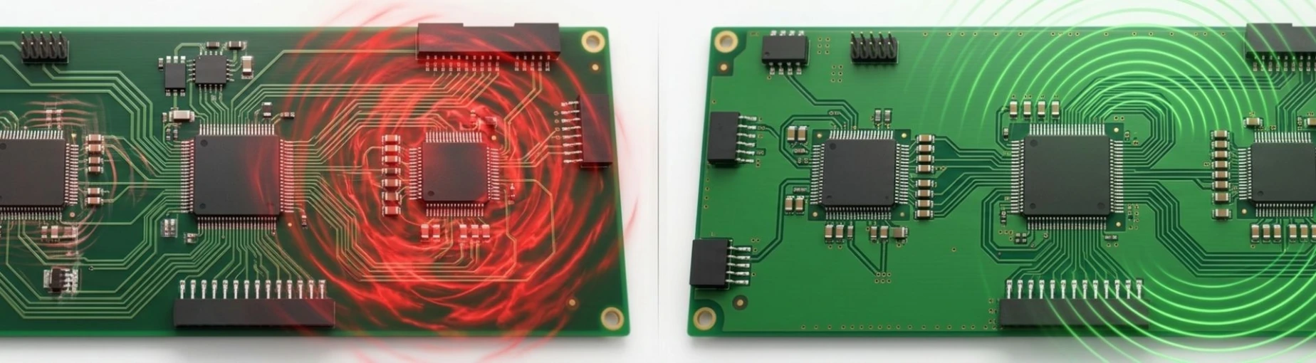
This is where Electromagnetic Interference (EMI) and Electromagnetic Compatibility (EMC) play a vital role. While these two terms are often mentioned together, they represent different aspects of electronic design. Understanding both concepts during PCB layout helps engineers improve signal integrity, reduce design issues, and build products that meet industry compliance standards.
In this article, we'll explain the difference between EMI and EMC, why they matter in PCB design, and the best PCB layout practices that help minimize interference while improving long-term product reliability.
EMI vs EMC: What's the Difference?
Although EMI and EMC are closely related, they are not the same. Understanding the distinction helps engineers make better design decisions throughout the PCB development process.

A simple way to understand the relationship is:
EMI is the interference. EMC is the ability to manage that interference successfully.
Reducing EMI is one of the most effective ways to improve EMC, which is why both concepts should be considered together during PCB design rather than as separate engineering tasks.
What Is Electromagnetic Interference (EMI)?
Electromagnetic Interference (EMI) is unwanted electromagnetic energy that disrupts the normal operation of electronic circuits. Whenever electrical current flows through a conductor, it creates an electromagnetic field. In modern high-speed electronics, these fields can interfere with nearby circuits, causing performance problems.
Poor EMI management can result in:
- Signal distortion
- Data communication errors
- Reduced signal integrity
- Random system resets
- Complete device malfunction
As electronic products continue to use faster processors and denser PCB designs, controlling EMI has become a critical part of every PCB layout.
Types of EMI
EMI generally appears in two forms.
Conducted EMI
Conducted EMI travels through electrical conductors such as:
- Power lines
- Ground connections
- Signal traces
Noise generated in one section of the circuit can easily spread to other components through these conductive paths.
Radiated EMI
Radiated EMI spreads through the air as electromagnetic waves. Long PCB traces, switching circuits, and RF components often act like antennas that either emit or receive unwanted electromagnetic signals.
Both types of interference can negatively affect circuit performance if they are not considered during PCB layout.
Common Sources of EMI in PCB Design
Several design factors contribute to electromagnetic interference.
Some of the most common sources include:
- High-speed digital circuits
- Clock oscillators
- Switching power supplies
- DC-DC converters
- Wi-Fi and Bluetooth modules
- RF communication circuits
- Poor grounding
- Long PCB traces
- Inadequate decoupling capacitor placement
- Crosstalk between adjacent signal traces
Although EMI cannot be completely eliminated, a well-planned PCB layout can significantly reduce its impact.
What Is Electromagnetic Compatibility (EMC)?
While EMI represents the interference itself, Electromagnetic Compatibility (EMC) refers to a product's ability to operate correctly without causing or suffering from excessive electromagnetic interference.
An EMC-compliant PCB should:
- Operate reliably in its intended environment
- Produce minimal electromagnetic emissions
- Resist interference from nearby electronic devices
Simply put, EMI is the problem, while EMC is the goal.
Designing with EMC in mind helps manufacturers produce reliable products that perform consistently under real-world operating conditions.
Why EMI and EMC Matter in PCB Layout
Ignoring EMI during PCB design often leads to expensive redesigns, failed compliance tests, and unreliable products.
A properly optimized PCB layout offers several advantages:
- Better signal integrity
- Stable electrical performance
- Improved product reliability
- Lower electromagnetic emissions
- Greater immunity to external interference
- Easier compliance with EMC standards
- Reduced manufacturing costs
- Higher long-term product quality
Addressing these factors early in the design process is far more effective than trying to solve EMI problems after PCB fabrication.
PCB Layout Mistakes That Increase EMI
Many EMI problems originate from simple layout mistakes.
Poor Ground Plane Design
A fragmented ground plane forces return currents to travel longer paths, increasing loop area and creating additional electromagnetic radiation.
Using a continuous ground plane provides a cleaner return path and significantly reduces noise.
Improper PCB Stackup
An unbalanced stackup affects signal integrity, impedance control, and electromagnetic performance.
Carefully arranging signal, power, and ground layers helps minimize EMI while improving electrical stability.
Long Signal Traces
Long traces can behave like antennas, allowing them to both transmit and receive unwanted electromagnetic energy.
Keeping critical signals short and direct reduces unwanted radiation.
Poor Return Current Paths
Every signal requires a return path.
If return currents are forced around plane splits or routing obstacles, electromagnetic emissions increase considerably.
Inadequate Power Filtering
Poor placement of decoupling capacitors allows switching noise to spread across the board.
Placing capacitors close to IC power pins helps suppress high-frequency noise before it affects other circuits.
Crosstalk Between Signals
Closely spaced parallel traces allow electromagnetic coupling between neighboring signals.
Maintaining proper spacing reduces crosstalk while improving signal integrity.
Best PCB Layout Practices for Better EMC
Achieving strong EMC starts with smart design decisions rather than relying solely on shielding after manufacturing.
Here are several proven PCB layout practices.
Design an Optimized PCB Stackup
A carefully planned stackup keeps signal layers adjacent to solid reference planes.
Benefits include:
- Lower loop inductance
- Better return current paths
- Improved impedance control
- Reduced electromagnetic radiation
Use Continuous Ground Planes
Solid ground planes help control return current flow and reduce radiated emissions.
Avoid routing high-speed signals across split ground planes whenever possible.
Minimize Loop Area
Large current loops generate stronger electromagnetic fields.
Keeping signal and return paths close together minimizes loop area and reduces EMI.
Keep High-Speed Signals Short
Short traces reduce:
- Signal reflections
- Propagation delay
- Radiation
- Noise pickup
Direct routing also improves overall signal quality.
Position Decoupling Capacitors Correctly
Place decoupling capacitors immediately adjacent to IC power pins.
This simple practice improves power stability while filtering high-frequency switching noise.
Use Via Stitching
Ground via stitching connects reference planes together and reduces electromagnetic leakage.
It also improves shielding in multilayer PCB designs.
Maintain Controlled Impedance
Controlled impedance routing is essential for:
- High-speed digital circuits
- RF designs
- High-frequency communication interfaces
Consistent impedance helps preserve signal quality while minimizing EMI.
PCB Layout Checklist for Reduced EMI
Before releasing your design for manufacturing, confirm that your PCB layout includes the following:
- Continuous ground planes
- Short high-speed traces
- Proper decoupling capacitor placement
- Controlled impedance where required
- Separation of noisy and sensitive circuits
- Small signal loop areas
- Complete Design Rule Check (DRC)
- Proper return current paths
Following this checklist greatly improves the likelihood of first-pass success.
How PCB Manufacturing Affects EMI Performance
Even an excellent PCB layout can experience performance issues if manufacturing quality is inconsistent.
Several fabrication factors influence electromagnetic behavior, including:
- Copper thickness
- Dielectric material consistency
- Layer alignment
- Controlled impedance accuracy
- Material properties
Working with an experienced PCB manufacturer helps ensure that the finished board performs exactly as intended.
As operating frequencies continue to increase, manufacturing precision becomes just as important as layout quality.
Common EMI and EMC Mistakes to Avoid
Many interference problems can be prevented with proper planning.
Avoid these common mistakes:
- Splitting ground planes beneath high-speed traces
- Routing signals across reference plane gaps
- Placing decoupling capacitors too far from ICs
- Ignoring return current paths
- Running high-speed traces in parallel for long distances
- Skipping Design for Manufacturability (DFM) reviews
- Assuming shielding alone will solve EMI issues
Correcting these issues early reduces development time and minimizes costly redesigns.
Final Thoughts
Although EMI and EMC are closely related, they serve different purposes in electronic design. EMI represents unwanted electromagnetic noise, while EMC ensures that electronic products can operate reliably without creating or suffering from excessive interference.
A carefully planned PCB layout remains the most effective way to control EMI and achieve better EMC performance. Practices such as proper grounding, optimized stackup design, controlled impedance routing, thoughtful component placement, and high-quality PCB manufacturing all contribute to a more reliable electronic product.
By considering EMI and EMC from the beginning of the design process, engineers can improve signal integrity, simplify manufacturing, reduce development costs, and build circuit boards that perform consistently in demanding applications.
Optimize Your PCB Layout with PCB Power
Creating reliable electronic products starts with a well-designed PCB layout backed by high-quality manufacturing. PCB Power provides end-to-end PCB solutions, including PCB layout support, PCB fabrication, PCB assembly, electronic component sourcing, and PCB stencil services to help engineering teams move smoothly from prototype to production.
Whether you're developing industrial equipment, automotive electronics, medical devices, or IoT products, PCB Power helps ensure your designs are optimized for performance, manufacturability, and long-term reliability.
Contact PCB Power today to discuss your next PCB project and request a customized quote.
Know More: https://pcbpower.us/blog/general-11/emi-vs-emc-pcb-design-47