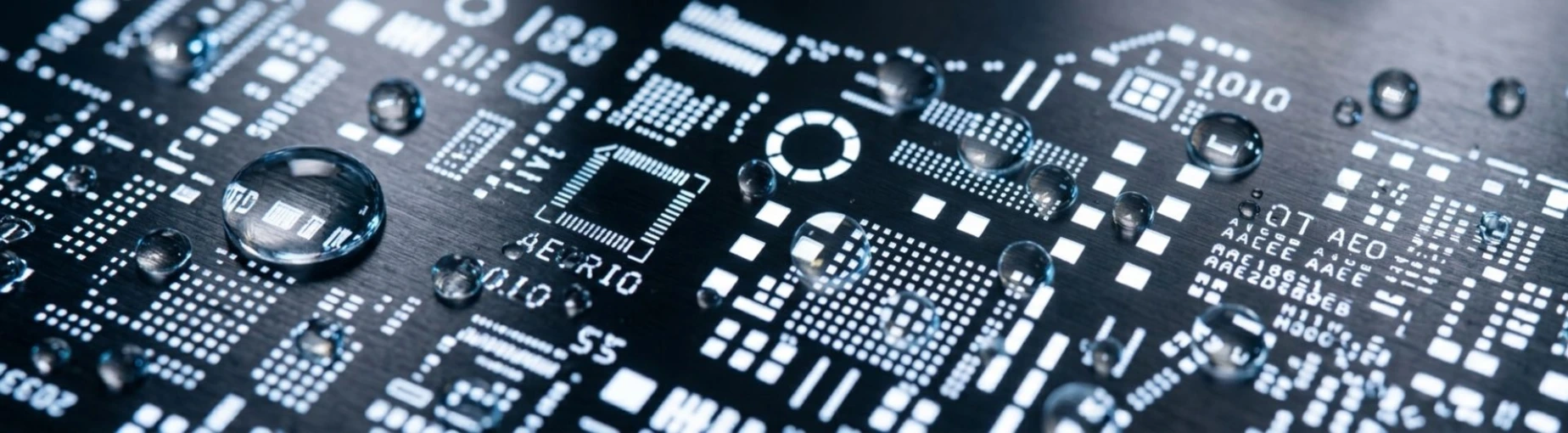
That is why selecting the right PCB Stencil Services is so important. As electronic devices become smaller and PCB layouts become more compact, manufacturers need stencil solutions that deliver accurate and repeatable solder paste deposition. One of the most effective ways to achieve this is by using nano-coated PCB stencils.
In this guide, we'll explain what nano-coated stencils are, how they work, their advantages, and when they make the most sense for your PCB assembly project.
What Is a Nano-Coated PCB Stencil?
A nano-coated PCB stencil is a standard laser-cut stencil treated with an ultra-thin protective coating after manufacturing. Unlike conventional coatings that mainly protect against corrosion, nano-coatings are designed to improve solder paste release during stencil printing.
The coating creates a smooth, low-friction surface that resists both moisture and solder paste buildup. Because solder paste is less likely to stick to the stencil walls, more paste transfers accurately onto PCB pads.
The coating is only a few nanometers thick, so it doesn't affect stencil dimensions or printing accuracy. Instead, it enhances stencil performance while maintaining precise aperture sizes.
Nano-coated stencils are commonly used for:
- Fine-pitch ICs
- Ball Grid Array (BGA) packages
- Micro-BGA components
- 0201 and 01005 passive components
- High-density SMT assemblies
- Complex multilayer PCBs
How Nano-Coating Improves Solder Paste Printing
During stencil printing, a squeegee forces solder paste through stencil apertures and onto PCB pads. Ideally, every aperture should release its entire paste volume.
In reality, some solder paste remains attached to the stencil walls due to friction and surface tension. As production continues, this residue can reduce printing consistency and create assembly defects.
Nano-coating lowers the stencil's surface energy, allowing solder paste to release more easily. The result is cleaner deposits and more consistent solder paste volumes throughout production.
Manufacturers benefit from:
- Better solder paste transfer efficiency
- Cleaner stencil apertures
- Uniform solder deposits
- Improved print repeatability
- Reduced stencil cleaning frequency
- Greater production consistency
Why Modern PCB Manufacturing Uses Nano-Coated Stencils
Today's PCB designs include increasingly smaller components with tighter spacing. As stencil apertures become smaller, solder paste release becomes more difficult.
Without proper stencil performance, manufacturers may experience inconsistent solder deposits that lead to costly rework or reduced product reliability.
Nano-coated stencils help maintain stable printing performance by reducing solder paste adhesion inside each aperture. This becomes especially valuable when assembling:
- Fine-pitch integrated circuits
- BGAs and micro-BGAs
- Miniature passive components
- High-density SMT boards
- Compact multilayer PCB designs
For manufacturers focused on quality and yield, improved stencil performance directly supports better assembly results.
Benefits of Nano-Coated PCB Stencils
Improved Solder Paste Release
The biggest advantage of nano-coating is improved solder paste transfer. More consistent paste release creates stronger and more reliable solder joints.
Fewer Assembly Defects
Better solder paste deposition helps reduce common PCB assembly problems, including:
- Solder bridging
- Insufficient solder
- Open solder joints
- Tombstoning
- Uneven paste deposits
Reducing these defects improves first-pass yield while minimizing rework.
Consistent Printing During Long Production Runs
Traditional stencils gradually accumulate solder paste residue, which affects print quality over time.
Nano-coated stencils stay cleaner for longer, helping manufacturers maintain stable print performance throughout extended production runs.
Reduced Cleaning Downtime
Because less solder paste sticks to the stencil surface, cleaning cycles become less frequent. This allows production lines to operate more efficiently with fewer interruptions.
Higher Manufacturing Yield
Consistent solder paste printing produces fewer defective assemblies. Better yields mean lower production costs, reduced scrap, and improved manufacturing efficiency.
Longer Stencil Performance
Although proper maintenance is still important, nano-coatings help reduce residue buildup and minimize wear caused by repeated cleaning.
When Nano-Coating May Not Be Necessary
Nano-coated stencils offer many advantages, but they aren't required for every PCB assembly project.
A standard laser-cut stencil often performs well when:
- Larger SMT components are used
- Component spacing is generous
- Production volumes are low
- Standard PCB designs are being assembled
- Existing printing processes already achieve reliable results
In these cases, stencil thickness, aperture design, solder paste selection, and printing process optimization often have a greater impact than nano-coating itself.
Nano-Coated vs Standard PCB Stencils
Choosing between a standard stencil and a nano-coated stencil depends on the application's precision requirements. While both are capable of producing reliable solder paste deposits, nano-coated stencils offer measurable advantages for complex assemblies.

Although nano-coated stencils require a slightly higher upfront investment, the improvement in print consistency and reduction in assembly defects often offsets the additional cost, particularly in medium- to high-volume production.
Choosing between a standard stencil and a nano-coated stencil depends on the application's precision requirements. While both are capable of producing reliable solder paste deposits, nano-coated stencils offer measurable advantages for complex assemblies.
When Should You Choose Nano-Coated PCB Stencils?
Nano-coated stencils are recommended when printing accuracy becomes critical.
They are especially useful for:
- Fine-pitch ICs
- QFP packages
- Ball Grid Arrays (BGAs)
- Micro-BGA packages
- 0201 and 01005 components
- High-density SMT assemblies
- Automotive electronics
- Aerospace applications
- Medical devices
- High-volume PCB manufacturing
For these products, even small variations in solder paste volume can affect long-term product performance.
Understanding the Limitations
Although nano-coating improves solder paste transfer, it is not a complete solution for every manufacturing issue.
Nano-coated stencils cannot compensate for:
- Poor PCB layout
- Incorrect stencil thickness
- Improper aperture design
- Low-quality solder paste
- Printer calibration issues
- Weak process control
Manufacturers should view nano-coating as one part of a well-optimized stencil printing process.
Choosing the Right PCB Stencil
Selecting the right stencil involves more than deciding whether nano-coating is required.
Engineers should consider several important factors, including:
- PCB complexity
- Component size
- Aperture geometry
- Stencil thickness
- Material selection
- Surface finish
- Production volume
- Required printing accuracy
Working with an experienced provider of PCB Stencil Services helps ensure the stencil is properly matched to the PCB design and manufacturing process.
Why Professional PCB Stencil Services Matter
Reliable stencil performance begins with proper engineering. Experienced PCB Stencil Services providers evaluate board design, manufacturing requirements, and assembly objectives before recommending the most suitable stencil solution.
For industries such as aerospace, automotive, industrial automation, robotics, IoT, and medical electronics, precision stencil design plays an important role in achieving consistent assembly quality and long-term product reliability.
Conclusion
As PCB assemblies become more compact and component sizes continue to shrink, solder paste printing becomes increasingly critical.
Nano-coated PCB stencils improve solder paste release, reduce printing defects, minimize cleaning downtime, and support higher manufacturing yields. While standard stencils remain suitable for many conventional applications, nano-coated stencils provide significant advantages for high-density, fine-pitch, and high-reliability PCB assemblies.
Choosing the right PCB Stencil Services partner ensures your stencil is designed for your specific PCB layout, production requirements, and quality expectations.
Whether you're building prototypes or scaling to mass production, investing in the right stencil solution helps improve assembly consistency, reduce rework, and deliver reliable electronic products.
Looking for Reliable PCB Stencil Services?
At PCB Power, we provide precision PCB Stencil Services along with PCB fabrication, PCB assembly, PCB layout, and electronic component sourcing under one engineering-driven workflow.
Whether your project requires a standard laser-cut stencil or a nano-coated solution for high-density PCB assembly, our experts can help you select the right stencil based on your design and manufacturing goals.
Get in touch with PCB Power today to discuss your PCB stencil requirements and request a customized quote for your next project.