While searching online, I found an awesome PCB project on Hackaday made by Giovanni from DesignLab, that I would like to share with maker.pro community. It’s basically a PCB lamp built from scratch.
Concept
One of the main purposes of this project was to give it a run to Neoden’s system. They have chosen the PCB lamp because it’s really easy to set it up. Almost everything was done through SMT.
Once the material was prepared and the process was clearly defined, they focused on sketches to come up with a minimalist, but clean design, that could be further developed
The manufacturing was broken down into 3 main processes: acrylic cutting & engraving, 3d printing & gluing and screws fastening,
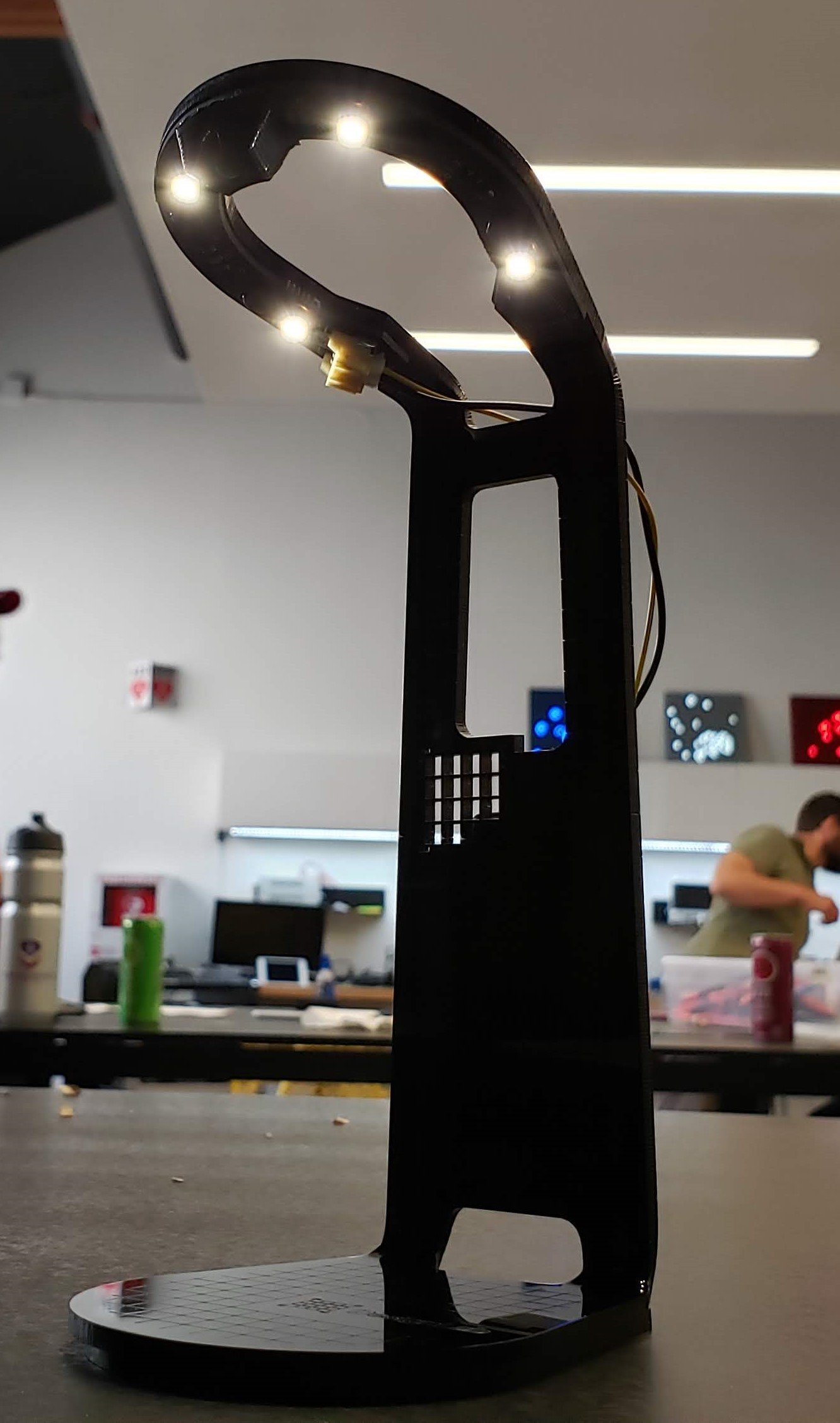
The most costly process is terms of time was the 3d printing, which took about 3 hours. The 3d printing was a necessity for the motion detector system which requested a component that blocks the LED from the sensor up to a certain distance. In terms of shape the lamp it’s looking more like an elevator, having the batteries placed on the back of it.
According to Giovanni, this was the most interesting part because both, engineers and designers were able to give their best together.
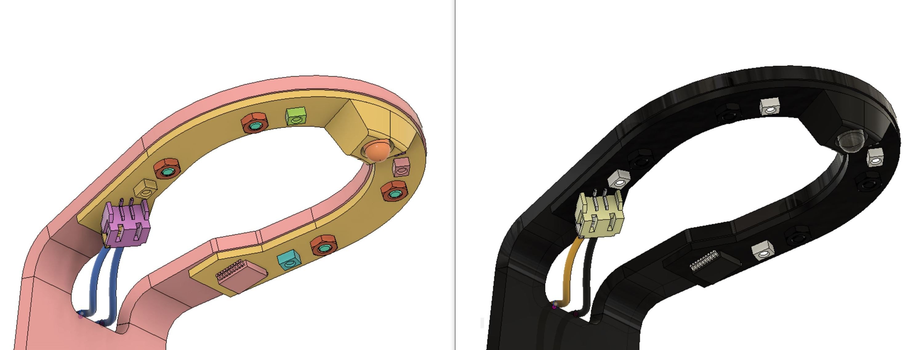
Giovanni stated: “Based on the design of the lamp, I shared with Voja a sketch with the ideal location of certain components on the PCB. I am not an electronic engineer, so there are many components I do not know we need and/or their location, therefore I try to keep my communication simple, detailing:
1.Basic shape or outline and assembly holes
2.Location of input/output components (LED's, connectors, power source, etc)
3.Other restrictions or requirements (light pipes, etc)
4.Everything else I assume is going to be populated with a bunch of resistors, capacitors, microcontrollers, etc.”
Assembly and manufacturing
The first PCB panels had a serious flaw - no extra spacing to the sides. “Erika improvised adapted and overcame the challenge by adding extra material to the sides in order to get us those badly needed 5 mm. Of course, this is a temporary fix and I just ordered new, improved boards today.”
The precision of the Neoden machine, it’s really good. The machine takes photos of the nozzle, board fiducials, grabs component, goes for another selfie and then flies over to the exact location where the component should be placed.
Management
For the management of this project they used a tool called Project Libre, which is simplified version of Microsoft Project.
What was left is manufacturing. “Erika has been hard at work programming the last pieces and running test boards. A great way to test boards and be able to recover most of the components is by using double sided tape on it."