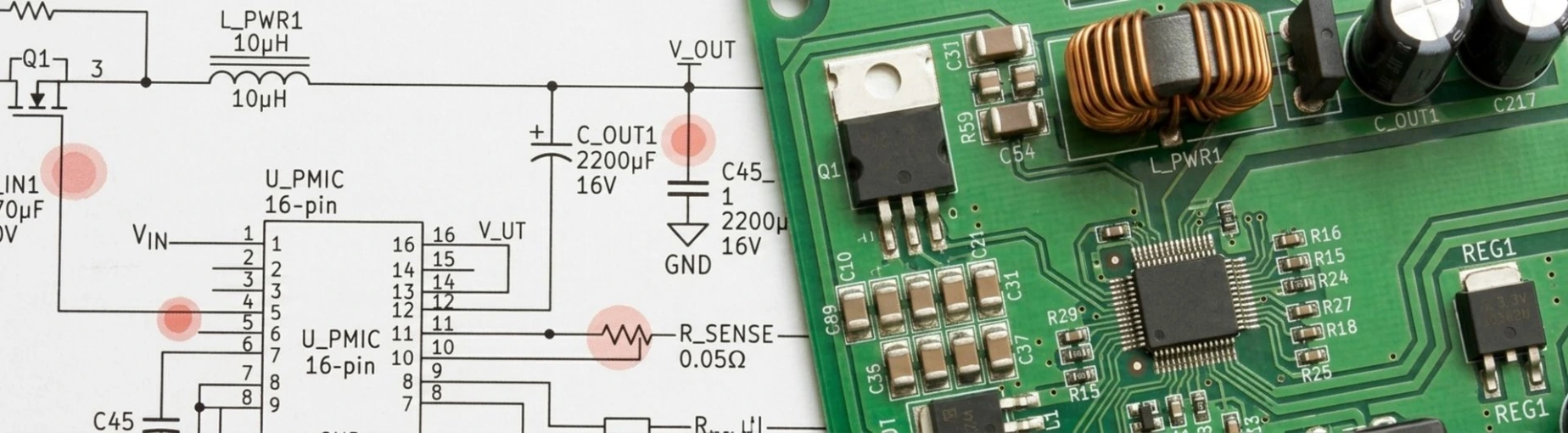
Although these terms are often used together, they serve very different purposes. Understanding the difference helps engineers build electronic products that are not only functional but also easy to manufacture and reliable in real-world applications.
Understanding the PCB Schematic
A PCB schematic is the logical blueprint of an electronic circuit. It shows how components such as resistors, capacitors, integrated circuits, and connectors are electrically connected. At this stage, the focus is entirely on the circuit's functionality rather than its physical appearance.
The schematic allows engineers to verify signal flow, confirm component selection, and ensure that the circuit performs as intended before moving into the physical design phase.
In simple terms, the schematic answers one important question: How should the circuit work?
What Happens During PCB Layout?
After the schematic is finalized, engineers begin the PCB layout process. This is where the logical circuit is transformed into a physical board that can be fabricated and assembled.
PCB layout involves placing every component on the board, routing copper traces, defining power and ground planes, and ensuring the design meets manufacturing requirements.
Unlike the schematic, PCB layout must consider practical engineering factors such as:
- Component placement
- Signal routing
- Power distribution
- Thermal management
- Electromagnetic interference (EMI)
- Manufacturing tolerances
A well-designed layout improves electrical performance while reducing production challenges.
Schematic vs. PCB Layout: Key Differences
Although both stages are part of the PCB design workflow, they have distinct objectives.

The schematic answers "How should the circuit work?", while the PCB layout answers "How can this circuit be manufactured reliably?"
This distinction is critical because even a perfectly designed schematic can result in a poorly performing product if the PCB layout ignores spacing requirements, routing constraints, thermal management, or signal integrity considerations.
Key Steps in PCB Layout Design
The layout process typically follows a structured workflow:
Import the schematic and netlist: The verified schematic is imported into PCB design software, preserving all electrical connections.
Define the board outline: Engineers establish the board dimensions, connector locations, mounting holes, and mechanical constraints.
Place components strategically: Critical components are positioned first to optimize signal flow and simplify routing.
Route copper traces: Electrical connections are converted into conductive pathways while maintaining proper spacing and trace widths.
Design power and ground planes: Dedicated planes improve signal integrity, reduce electrical noise, and provide stable current paths.
Perform design verification: Design Rule Checks (DRC) identify spacing violations, routing issues, and manufacturing conflicts before production begins.
Generate manufacturing files: Gerber files, drill data, bill of materials (BOM), and assembly documentation are prepared for fabrication and assembly.
Best Practices for Reliable PCB Layout
Successful PCB designs follow several proven practices:
- Keep signal paths as short as possible.
- Group related components together.
- Maintain continuous ground planes.
- Consider heat dissipation during component placement.
- Design with manufacturing requirements in mind.
- Verify the design thoroughly before fabrication.
These practices help improve board performance while minimizing production errors.
Common Design Mistakes to Avoid
Even well-designed circuits can experience problems if the PCB layout is not carefully planned.
Some common mistakes include poor component placement, fragmented ground planes, excessive use of vias, ignoring manufacturing clearances, and skipping final design verification.
Addressing these issues early helps reduce redesign costs and shortens product development timelines.
Why PCB Layout Is So Important
PCB layout directly affects every stage of manufacturing. A clean and optimized layout improves fabrication accuracy, simplifies automated assembly, enhances solder quality, and increases overall product reliability.
Engineers who consider fabrication and assembly requirements during the layout stage often achieve better production yields and fewer manufacturing issues.
Companies like PCB Power provide complete PCB solutions that support businesses throughout the product development process—from PCB layout and fabrication to assembly and component sourcing—helping transform circuit designs into production-ready electronic products.
Final Thoughts
A PCB schematic defines how an electronic circuit should function, while the PCB layout determines how that design becomes a manufacturable product. Both stages are equally important, and success depends on careful planning, accurate design practices, and thorough verification.
Investing time in an optimized PCB layout not only improves electrical performance but also simplifies fabrication, reduces production costs, and creates reliable electronic products that perform consistently in the real world.
Know More: https://www.pcbpower.us/blog/general-11/schematic-to-pcb-layout-process-51