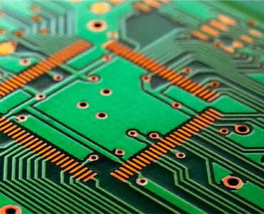
Understanding vdd vs vcc helps designers interpret power requirements, avoid incorrect connections, and organize power distribution across a circuit board.
This article explains the difference between VDD and VCC, their practical applications, and how these supply references influence PCB layout decisions.
What Do VDD and VCC Mean in Electronics?
VDD and VCC are conventional labels used to identify supply voltages in electronic circuits. Their origins are associated with different transistor technologies.
What Is VDD?
VDD stands for drain supply voltage and originates from Metal-Oxide-Semiconductor Field-Effect Transistor (MOSFET) terminology.
It commonly identifies the positive supply connection in CMOS-based devices, including microcontrollers, memory chips, digital processors, and other integrated circuits.
What Is VCC?
VCC refers to the collector supply voltage, a naming convention originating from Bipolar Junction Transistor (BJT) circuits.
It is frequently found in TTL logic devices, analog electronics, communication modules, and legacy circuit designs.
However, modern manufacturers may use either label regardless of the internal transistor technology. The component datasheet remains the authoritative reference.
VDD vs VCC: Understanding Their Key Differences
The primary distinction between these supply labels concerns their historical origins and common applications rather than an inherent difference in voltage.

The difference between VDD and VCC becomes particularly important when a PCB contains devices operating at multiple voltage levels.
For example, a microcontroller may require 3.3 V at its VDD pins, while a connected peripheral uses 5 V at a pin labelled VCC.
These connections should not be combined without verifying voltage compatibility.
For a more detailed technical explanation, PCB designers can refer to this guide on VDD vs VCC and their electrical differences.
Why Does the Difference Between VDD and VCC Matter in PCB Layout?
PCB layout involves more than placing electronic parts and connecting copper traces. Designers must ensure that each integrated circuit receives the required voltage while maintaining acceptable noise, temperature, and signal performance.
Understanding the difference between VDD and VCC helps prevent mistakes in the power distribution network.
Incorrect supply connections may cause unstable operation, communication errors, excessive current consumption, or permanent damage to sensitive electronic devices.
Power Rail Identification
Each power net should have a clear name that reflects its function and voltage requirements.
Labels such as 3V3_DIGITAL, 5V_ANALOG, and VDD_CORE make circuit documentation easier to interpret and help reduce accidental connections between incompatible voltage domains.
Voltage Compatibility
Designers must verify recommended operating voltages, maximum ratings, and interface requirements before connecting devices.
A shared voltage rail is appropriate only when the connected components and the overall circuit architecture support it.
How to Manage VDD and VCC Connections During PCB Design
A practical approach to vdd vs vcc requires careful consideration of component specifications, copper routing, grounding, and local power stability.
1. Verify Power Pins Using Datasheets
Before creating a PCB layout, review each component's pin configuration and electrical characteristics.
Check whether the device requires separate supplies for its core, input/output interfaces, or analog circuitry. Different supply pins may require different voltage levels or filtering arrangements.
2. Position Decoupling Capacitors Correctly
Integrated circuits generate transient current demands during switching.
Decoupling capacitors placed close to supply pins help reduce voltage fluctuations and high-frequency noise.
Keep capacitor connections short, maintain a low-inductance return path, and follow the manufacturer's recommendations for capacitance values and placement.
3. Design Appropriate Power Distribution Paths
Power traces and copper planes must support the expected operating current.
Consider trace width, copper thickness, voltage drop, thermal performance, and available PCB layers.
For designs with higher current requirements, wider copper connections or dedicated power areas may provide better distribution than narrow traces.
4. Maintain Reliable Ground References
VDD is commonly paired with VSS, while VCC may appear alongside GND or VEE.
However, these naming conventions do not automatically establish whether the associated references are electrically identical.
A continuous ground reference and carefully planned return paths can reduce unwanted noise and electromagnetic interference.
5. Validate the Final PCB Layout
Perform electrical rule checks, design rule checks, and a review of power-net assignments before fabrication.
These checks can identify unintended connections, inadequate clearances, and routing issues that might affect circuit performance.
5 Common VDD and VCC Mistakes to Avoid
Recognizing the difference between VDD and VCC is especially useful when reviewing designs containing multiple integrated circuits.
Common errors include:
- Assuming both labels always indicate identical voltage levels.
- Connecting separate power domains without checking datasheets.
- Placing decoupling capacitors too far from supply pins.
- Using insufficient copper width for current requirements.
- Overlooking supply pin connections during schematic-to-layout verification.
Addressing these issues during design review can reduce unnecessary PCB revisions and troubleshooting during prototype testing.
Final Thoughts
Understanding vdd vs vcc supports accurate schematic interpretation and effective power distribution planning.
While both terms commonly indicate supply connections, their actual electrical requirements depend on the devices and circuit architecture.
The difference between VDD and VCC should therefore be evaluated through component specifications rather than naming conventions alone.
For engineers preparing a PCB design for fabrication, PCB Power provides additional technical guidance in its VDD and VCC comparison guide. Reviewing these fundamentals alongside component requirements can help establish a more consistent PCB layout and verification process.