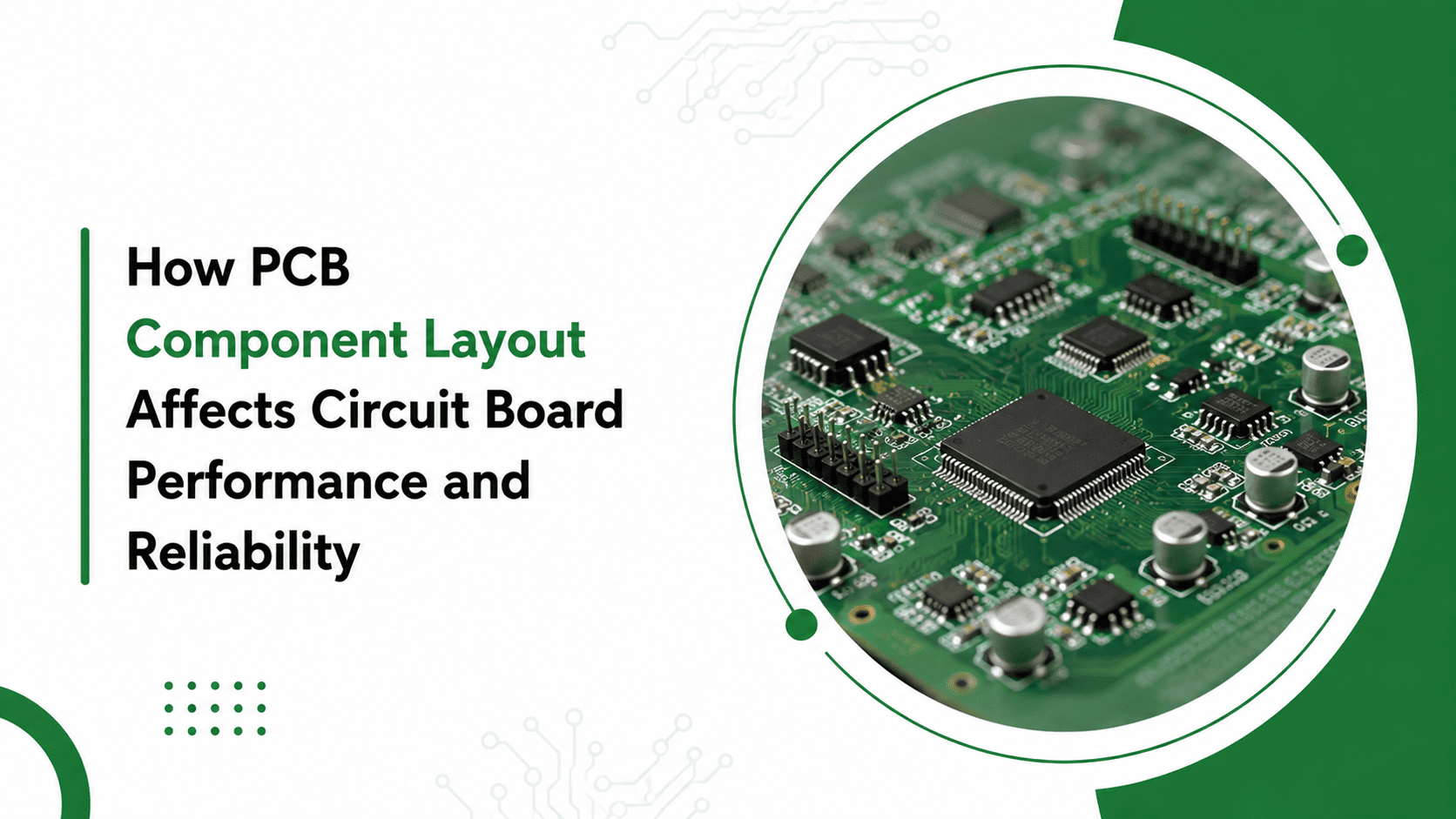
One of the most important factors influencing the success of any electronic product is pcb component layout. The placement of components on a PCB directly impacts electrical performance, thermal behavior, manufacturability, and long-term reliability.
Whether you're developing a simple consumer device or a complex industrial system, understanding the relationship between component placement and board performance can help prevent costly design issues later in the development cycle.
What Is PCB Component Layout?
PCB component layout refers to the process of positioning electronic components on a printed circuit board before routing begins. It serves as the foundation for a successful PCB design because every placement decision affects signal flow, thermal management, assembly efficiency, and overall product performance.
A well-planned layout helps engineers:
- Improve signal integrity
- Reduce electrical noise
- Optimize heat dissipation
- Simplify manufacturing
- Enhance product reliability
Poor placement decisions, on the other hand, can lead to performance problems that are difficult and expensive to correct later.
Why Component Placement Matters
Many PCB performance issues can be traced back to layout decisions made early in the design process.
Proper component placement helps ensure:
- Efficient current flow
- Stable signal transmission
- Balanced thermal distribution
- Easier assembly processes
- Reduced electromagnetic interference (EMI)
As modern electronic devices become smaller and more powerful, effective placement strategies become increasingly important.
The Connection Between Circuit Board Components and Performance
Every electronic product contains a combination of active and passive components working together to perform specific functions.
Common circuit board components include:
- Resistors
- Capacitors
- Integrated circuits (ICs)
- Connectors
- Inductors
- Sensors
The way these components are arranged affects how efficiently signals travel across the board and how well the system performs under real-world operating conditions.
For example, placing high-speed components too far apart can increase signal delays, while poor placement of power components may create thermal hotspots.
Signal Integrity Starts with Layout
Signal integrity refers to the quality of electrical signals as they travel through a PCB.
As operating frequencies continue to increase, layout decisions play a critical role in maintaining reliable signal transmission.
Some common signal integrity challenges include:
- Crosstalk
- Signal reflections
- Electromagnetic interference
- Timing mismatches
To minimize these issues, designers often:
- Keep critical traces short
- Place related components close together
- Maintain proper grounding
- Reduce unnecessary routing complexity
Good layout practices help ensure that signals reach their destination accurately and consistently.
Thermal Management and Component Placement
Heat is one of the most common causes of electronic reliability problems.
Certain pcb components, such as processors, power management devices, and voltage regulators, generate significant amounts of heat during operation.
Strategic placement can help improve thermal performance by:
- Separating heat-generating components
- Allowing better airflow
- Supporting heat sink installation
- Reducing localized temperature buildup
Thermal considerations should be addressed during the layout stage rather than after a prototype has been built.
Design for Manufacturability (DFM) Considerations
A PCB design may work perfectly in simulation but still create manufacturing challenges if component placement is not optimized.
Design for Manufacturability (DFM) focuses on creating layouts that can be fabricated and assembled efficiently.
Key placement considerations include:
- Adequate spacing between components
- Proper orientation for automated assembly
- Accessibility for inspection and testing
- Sufficient clearance around connectors and mechanical features
Considering manufacturability early helps reduce production delays and improve assembly yields.
Common PCB Component Layout Mistakes
Even experienced designers occasionally encounter layout-related issues.
Some common mistakes include:
Placing Components Too Close Together
Overcrowding can create thermal problems, complicate assembly, and increase the risk of manufacturing defects.
Ignoring Signal Paths
Poor placement may force longer routing paths, increasing resistance and degrading signal quality.
Inadequate Grounding Strategy
Improper placement of ground-related components can introduce noise and affect system stability.
Overlooking Thermal Zones
High-power components grouped together can create excessive heat concentration.
Failing to Consider Future Assembly
Ignoring assembly requirements during layout can lead to manufacturing challenges and increased production costs.
Best Practices for Reliable PCB Layout
To improve performance and reliability, designers should follow several proven layout principles:
- Place critical components first
- Group related circuits together
- Minimize high-speed signal path lengths
- Separate analog and digital sections where appropriate
- Plan thermal management early
- Consider manufacturing requirements during placement
- Perform DFM reviews before production
These practices help create designs that perform reliably throughout the product lifecycle.
Why Component Selection and Placement Work Together
Component selection and component placement are closely connected. Even high-quality parts may not perform optimally if they are placed incorrectly.
Engineers should evaluate both the electrical characteristics and placement requirements of selected components during the design process.
Understanding the functions and characteristics of various components can significantly improve layout decisions and overall product performance. For readers interested in learning more about component selection, this guide on circuit board components provides a useful overview of common component types and their applications.
Conclusion
PCB performance depends on more than the quality of individual components. The way those components are arranged on the board plays a major role in determining signal integrity, thermal performance, manufacturability, and long-term reliability.
A thoughtful pcb component layout strategy helps engineers avoid common design challenges while improving product quality and production efficiency. By considering signal flow, thermal management, and manufacturing requirements early in the design process, teams can create more reliable and scalable electronic products.
As electronic systems continue to become more complex, effective component placement will remain one of the most important factors in successful PCB design.