Now that you've been introduced to the two Panelization methods, let's dive in depth to the V-groove method!
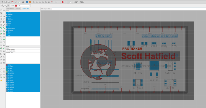
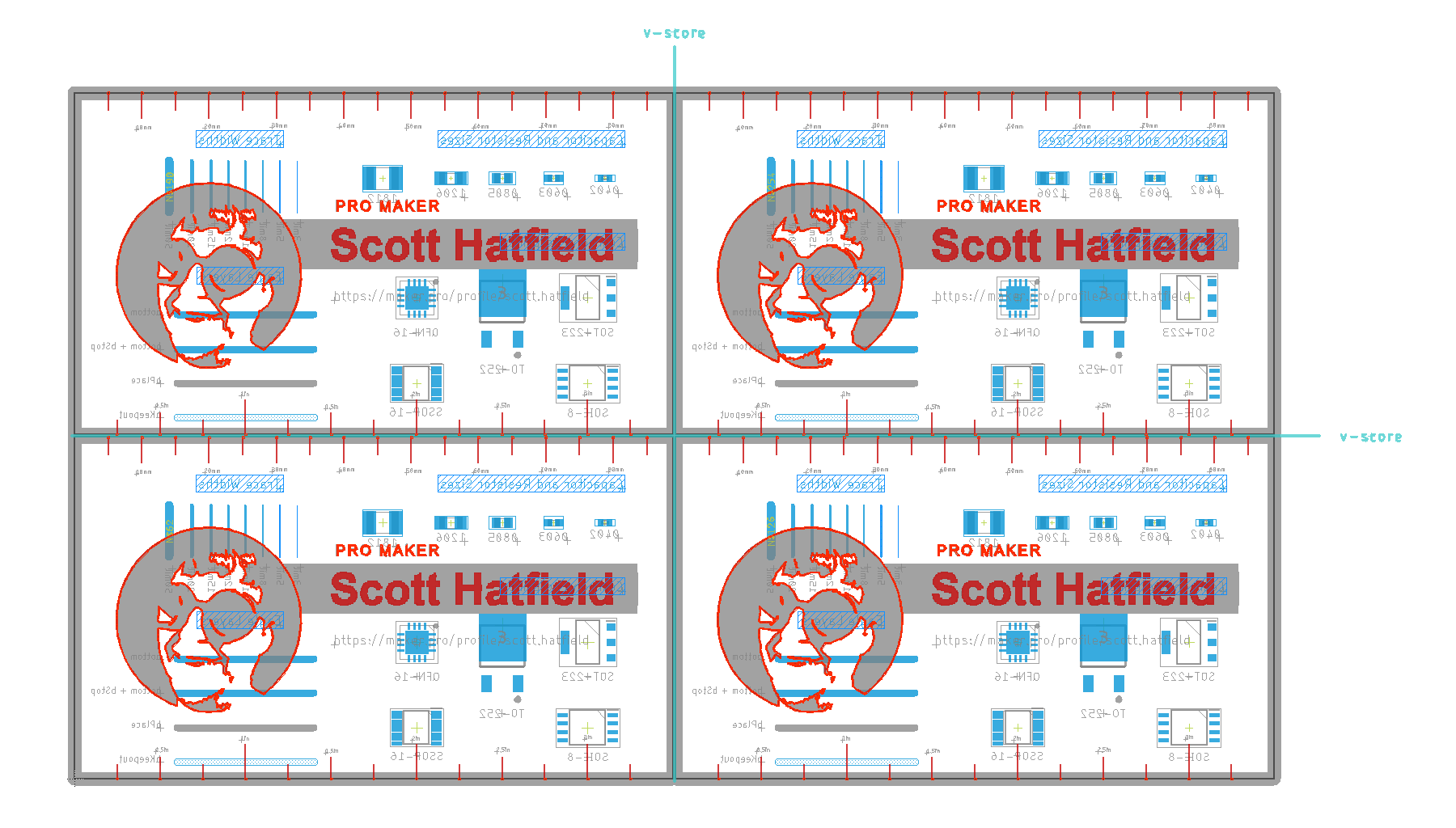
In this BRD design file in Autodesk EAGLE, you can see the V-groove lines in a teal color
Since the V-groove itself is created with a saw blade, this panelization method can only be used in designs in which the individual PCBs can be separated by straight lines that extend from once side of the panel to the other.
Getting Started With V-groove Panelization
Before we get started on panelizing PCBs in Autodesk EAGLE, one important note is that you cannot simply copy/paste your designs to create a panel. The issue is that when you copy a board and paste a second one, EAGLE will automatically update all the part and trace names to avoid duplication. So, every copy of the board will have different part designators. This causes a big problem for getting your boards assembled because the bill of materials you supply your manufacturer will be accurate for the first version of your PCB but it will be wrong for every subsequent copy.
When the PCB is simply copy/pasted from the bottom board to the top, EAGLE automatically changes all of the part names
Therefore, we will use a user language program (ULP) to copy your board without changing any of the designators.
Step 1: Download the SparkFun ULP Repository
The tool we will use to create the panel is a ULP from SparkFun called SparkFun-Panelizer.ulp. This ULP was created by SparkFun to allow their design team to more easily create V-groove panels for their products. The ULP can be downloaded from SparkFun’s EAGLE settings repository on GitHub. To make the ULP work correctly, we will need a few other files from the repository, so just download the entire thing.
Step 2: Set Up the ULP
We will need to move a few files from the downloaded repository into EAGLE’s directory on your computer to get the SparkFun-Panelizer.ulp script to work correctly.
First, move the SparkFun-Panelizer.ulp file from the \ulp directory in the repository into the Eagle \ulp directory. This is typically located in \Documents\eagle\ulps.
Second, move all the DRU files from the \dru directory in the repository into the \design rules directory in your EAGLE installation. This is typically located in \Documents\eagle\design rules.
Step 3: Run the ULP
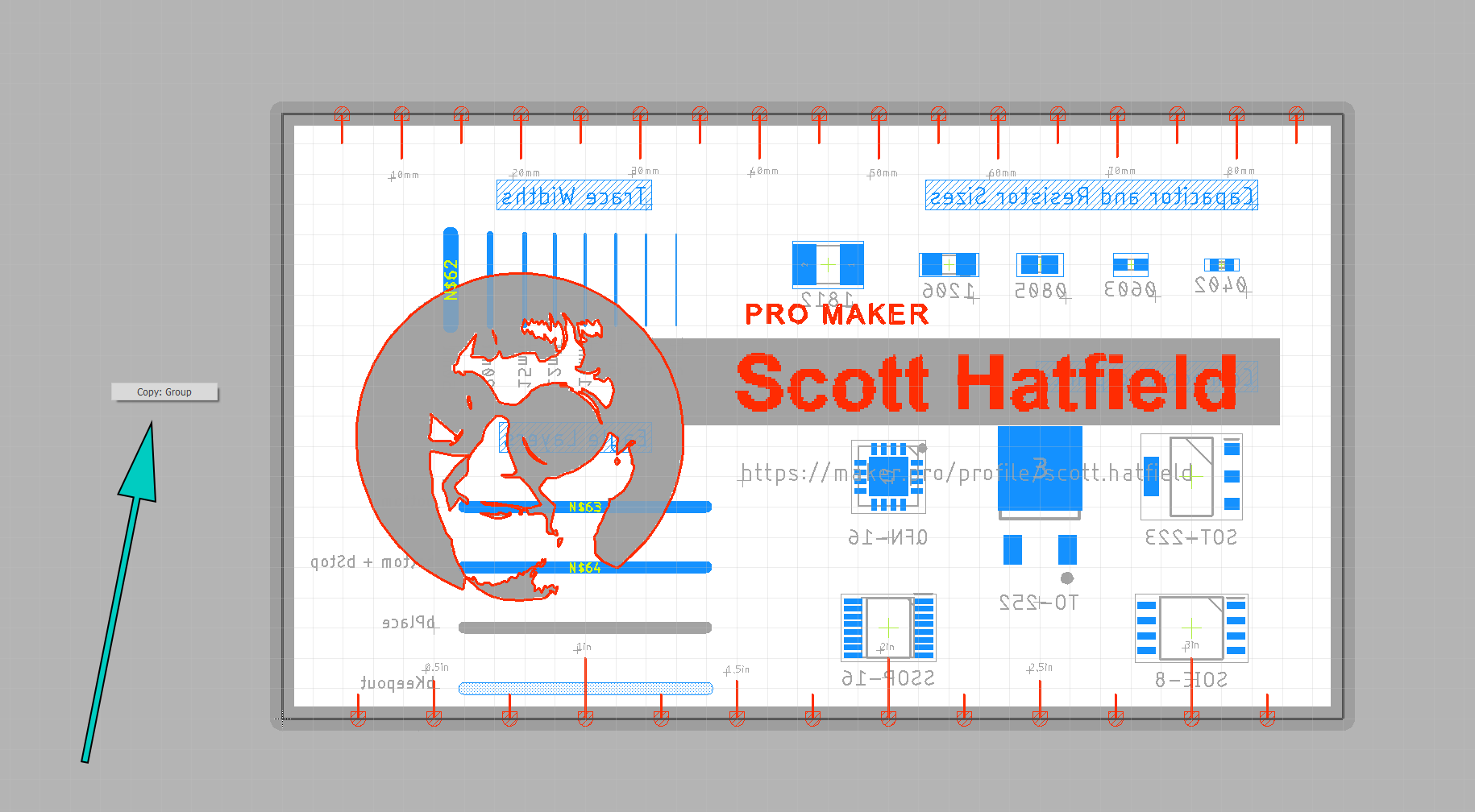
With the SparkFun-panelizer.ulp script loaded in your EAGLE installation directory, we can get to work actually using it to penalize a BRD file. The first step is to copy (but not paste) your PCB design. With your BRD file open, and all layers visible, use the group select tool to select the entire design.
Use the Group tool to select the entire design.
Then, using the Copy tool, right click anywhere on the design, and select Copy: Group. This will place a copy of all the visible layers on the clipboard. However, do not paste the design.
Next, at the top of the screen, click the ULP button. This will open a dialog box used to select a ULP to run. Here we will be using the ULP we downloaded earlier, so, to select that script, click the Browse button.
From the EAGLE installation directory where you placed the SparkFun-Panelizer.ulp file earlier, usually \Documents\eagle\ulps, select the SparkFun-Panelizer.ulp.
Select the SparkFun-Panelizer.ulp script from your EAGLE installation directory
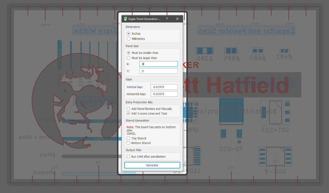
When you open the ULP, EAGLE will present a dialog box for configuring the script. Here is where we will need to do a bit of simple math to figure out how many copies of the board to create. You could approach this issue in a couple different ways:
- If you are interested in simply maximizing the number of PCBs you are able to fit in the largest panel on offer from your PCB manufacturer, start by selecting the “Must be smaller than” checkbox from the Panel Size area of the dialog box. Then, look up the panel specifications for your PCB manufacturer and input their maximum panel size. This will make the ULP create as many copies of your board as will fit in this maximum panel size. Note that some manufacturers will charge extra beyond a certain number of copies of your PCB.
- If you want to make a certain number of copies of your PCB, there will be just a little calculation required. You will need to calculate a panel size that will accomodate the number of boards you need, plus the margin between boards needed for the V-groove. To do this, multiply the width of your board by the number of boards you want across your panel. Add 0.01575 inches per board for the space between them. This will be the width of your panel. Similarly, multiply the height of your board by the number of boards you’d like in the y-direction on your panel and again add 0.01575 inches per board. This is the height of your panel.
When you’ve entered your X and Y values depending on the number of boards you need, press the Generate button. You will end up with an array of PCBs divided by V-groove lines on the Milling layer.
The ULP will create an array of PCBs separated by V-groove lines.
Step 4: Send to your Manufacturer
At this point, your design is ready to be sent for manufacturing. Depending upon the requirements for your manufacturer, you may be able to upload the EAGLE BRD file directly (this is the case with OSH Park), or you can use the CAM processor in EAGLE to create Gerber files.
Create Gerber Files
The majority of PCB manufacturers require Gerber Files to make your boards. Gerber files are a universal standard for manufacturing PCBs. The files themselves generate as a set of files, each containing different information about your design. To create Gerber files in Autodesk EAGLE, start by clicking on the CAM Processor tool at the top of the page.
For Seeed Studio Fusion PCB, there is a CAM profile built into EAGLE. In the CAM Processor dialog box. To access the profile, choose Load job profile > System Examples > Third Party > Seeed Fusion > SeeedFusion_2_layer.cam.
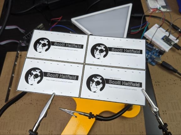
Once the panels arrive, the V-grooves in the board that separate the individual PCBs make the boards easy to snap apart, as long as you take some care not to put too much stress on the board.
V-groove Panelization Recap
Of the two major methods of panelizing PCBs, V-groove and tab-route, V-groove is the simplest and cheapest method. In V-groove panels, a saw is used to cut part way through each side of the PCB between individual boards. The resulting thin section of FR-4 is strong enough for the panel to remain intact throughout the assembly process, but it is weak enough to separated with relative ease.
V-groove panelization is feasible for panels in which the individual PCBs can be separated by straight lines that extend all the way across the panel. For more complex shapes, tab-route panelization, in which boards are separated by a gap created by a CNC mill, is needed.