Part two of a series on how to build your own computer from scratch, based around the Z80 CPU.
In this series, Robin builds a Z80 computer from scratch. Catch up with these posts:
In the last Z80 project, we learned about the Z80 CPU and how some of its input/output pins work. In this episode, we will add memory to our machine and look into memory structures for computers.
Introduction to Memory
Computers have the ability to perform many operations and conditional instructions in the blink of an eye—but these operations are normally useless on their own. If these instructions are sequentially combined with other instructions, the result is a program that can be made to do just about anything (assuming no limitations on IO).
Our Z80 CPU from the last project was able to execute instructions by setting the DIP switches on the databus to specific values but this means that, for the Z80 to execute multiple instructions, the switches would have to be changed every single time. This is where memory comes in!
Memory in a computer can be thought of as a large table with the first column containing an address (number in the list), and the second column containing information. This information could be anything including a specific instruction, a number, or even a letter. As the computer runs, it will go to this table and pick a specific row and either read or write to the data column.
In real life, memory typically comes in two forms; RAM and ROM. RAM in a computer stands for Random-Access-Memory and can be read from and written to. ROM in a computer stands for Read-Only-Memory and this can only be read from (not written to). ROM will typically be used to store a bootloader which is a small piece of code designed to load a much bigger program (such as an OS) into RAM via an external memory device (hard disk, USB drive, etc.).
Memory ICs will typically have the following IO pins:
- Address Pins (Ax) – These point to a specific row in the memory table
- Data Pins (Dx) – These pins are used for data (reading/writing) found at the address Ax
- CS – Stands for Chip Select and enables the IC. Active low
- OE – Stands for Output Enable and allows external devices to read data. Active low
- WE – Stands for Write Enable and writes data. Active low
The pinout for a typical RAM IC (Cypress CY62256N)
While many different varieties of RAM exist, we will explicitly be using SRAM and there is a good reason for this! RAM is a very generic term and covers most volatile memories available for computers. They are called volatile because they lose all their stored information as soon as the power is disconnected.
The most common type of RAM is called DRAM, which stands for Dynamic RAM. Each data bit inside the memory uses a capacitor that can either be charged or discharged. While this sounds like a great idea, the capacitor very quickly discharges and thus loses the information stored on it, which is why DRAM requires constant refreshing. This refreshing cycle can be very complex and usually requires external circuitry to handle this.
To make our lives easier, we will be using SRAM, which stands for Static RAM. It, too, is volatile and will lose the stored information when the power is disconnected; but, unlike DRAM, it does not need refreshing. Instead, each data bit in SRAM can be thought of as a flip-flop with data and clock lines. These latches are bi-stable and so are stable in both 0 and 1 conditions.
SRAM bits, however, take up more silicon than DRAM and are therefore smaller in size (MB as opposed to GB)—and also more expensive. Luckily for us, small SRAM parallel ICs (a few KB in size) only cost a buck or two and are available in DIP packages!
DRAM Cell (left) and a SRAM cell (right)
The Cypress CY62256NLL 32KB 8 Bit Parallel SRAM
Reading and Writing Memory
While all of this may seem complex and difficult to understand, reading and writing to/from memory could not be easier!
When not doing anything with the memory, ensure the following:
- CE, OE, and WR are 1 (typically 5V)
- Address pins don’t matter!
- Data pins don’t matter!
To read the data found at address Ax:
- Set the address pins to the location that you want to read
- Ensure that the data bus is not being driven (i.e., floating)
- Set CS to 0 (to enable the chip)
- Set OE to 0
As soon as OE goes low, the data found at address Ax will appear on the data pins and can be read by any digital logic circuit including the Z80 CPU and microcontrollers.
To write data to address Ax ...
- Set the address pins to the address Ax
- Set the data pins to the data that you want to store (GND for 0 and VCC for 1)
- Set the CS pin low to enable the memory
- Toggle WE low then high to write the byte
But how do we connect a memory IC to a Z80 CPU? What circuitry do we need to make to get the reading and writing to work?
As it turns out, memory read and write cycles are essentially industry standard with most memory ICs working in the same way. And the memory access on the Z80 is no different—it can be directly connected to a memory IC!
- Z80 RD connects to memory OE pin
- Z80 WR connects to memory WE pin
- Z80 MREQ connects to memory CE pin
- Z80 Address pins connect to memory Ax pins
- Z80 Data pins connect to memory Dx pins
RAM and ROM
While the Z80 can be directly connected to a memory IC it is not entirely desirable for one reason; RAM and ROM! When the Z80 first turns on it starts executing instructions found at address 0 and if our computer only has SRAM then the data that the Z80 will read from the memory will be garbage as the SRAM is volatile and any instructions that we program in are lost when the computer is turned off and on again (a hard reset). If our computer only has ROM then the Z80 would read instructions programmed into the ROM (even if the power has been turned off). However, as soon as the Z80 needs to store something into memory it won’t be able to as the memory is read-only and will therefore crash the program. We need to find away of combining both a ROM and SRAM IC so that both can be accessed by the Z80 but not at the same time as that would cause bus collisions (i.e. two ICs enabled at the same time may both try to access a common bus). The solution is memory organization and in our computer this is done with a single IC; the 74139. This IC is a de-multiplexer which takes in two binary bits and will produce one of four possible outputs.
By connecting A0 to the Z80s A8 pin and the E0 pin to the Z80s MREQ pin we get two memory banks. When the Z80 is accessing memory locations lower than 256 (0x0100) the A8 pin will be low and this will result in O0 being low and O1 being high. When the Z80 accesses memory addresses higher than 255 (0x00FF) the A8 pin will be high and this will result in O0 being high and O1 being low. If we then connect the ROM CS to O0 and the SRAM CS to O1 the result is a Z80 system that can access both ROM and RAM.
Testing
Testing this computer is tricky if the ROM has no program put onto it. In next Z80 project in our series, we'll learn how to build your own EEPROM programmer so you can load your basic ROM programs. To confirm your machine is running correctly, check the MREQ lines, the address lines, and the CS lines.
Read More
Construction
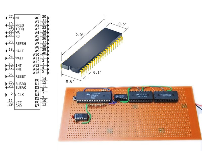
This project can be built using most, if not all, circuit construction techniques. But, for the sake of expansion and modification, I have chosen to use a commonly available stripboard. This stripboard is particularly useful as it has many power rails and separated short tracks that work well with DIP packages.
Wiring the computer is done on two layers: the top layer, which is control signals only, and the bottom layer, which is address and data signals only. This separation makes it easier to track down control signals which are typically the cause of many issues.
The underside of the Z80 project before wiring
Control wires on the top side use different colors to help identify the different functions. For example, this computer uses:
- Green wires for clock and chip select lines
- Purple for MREQ
- Grey for RD
- Orange for WE
It should also be noted that the ROM has its WE pin connected to 5V as it will not be used for writing data to (remember, its Read-Only-Memory).
The control wires on the top side
The underside wiring is done with copper magnetic wire, which is solderable. This wire is very thin (0.3mm) and is coated with an enamel that acts as an insulator. This enamel is also solderable, which means that the pad with solder is heated first, then the wire is inserted into the molten solder which binds the wire to the pad.
You should be ready to get started on the memory for your Z80!
You can see me work on this portion of the project in the video below: