Every engineer knows that IC packaging plays an important role in design, but making the right choice for a project can become overwhelming with so many options available. And with so many new packaging designs, it can be hard to tell which one has the right combination of benefits and features.

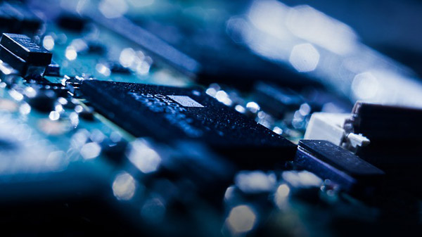
Computer components form one area where integrated circuit packaging innovations are key. Pictured: a close-up of the components of a computer processor. Image Credit: Pixabay.
Goals of Integrated Circuit Packaging
The main goals of IC packaging are to prevent damage to the IC, protect it from corrosion, and mount the electrical contacts in a manner that is compact and compatible with existing electronic components and devices. In addition, lower cost, power management, and high reliability have always been important factors in IC packaging.
There are secondary goals to packaging, too, however. For example, the increased integration of chip functions into a single package is becoming increasingly important. This approach typically reduces costs while also allowing certain chips, such as memory and processing chips, to be brought closer to each other and result in reduced latency. In fact, reduced latency leads directly into another major driver behind modern IC packaging: improved performance.
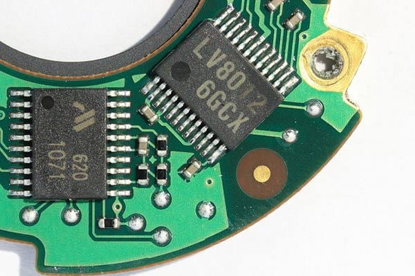
A printed circuit board (taken from a Canon digital camera), whose two exposed chips are manufactured using traditional methods. Image Credit: Pixabay.
Innovative Approaches to Integrated Circuit Packaging
There have been numerous advancements made relative to IC packaging, typically driven by the fact that more traditional approaches are proving more expensive per node and unwieldy for use with state-of-the-art electronics. Some of the newer innovations in IC packaging are fan-out, 2.5D, 3D, and hybrid bonding.
Fan-Out Integrated Circuit Packaging
Fan-out design approaches the said packaging challenges by integrating dies and components in a single, wafer-level package. The original fan-out design was referred to as embedded wafer-level ball-grid array (eWLB). While eWLBs are limited to fewer than 500 I/Os, modern fan-out designs support more than 500 I/Os. The major drawbacks of fan-out chip packaging is the cost and die shift; however, many consumers find themselves confused by the multiplicity of the various fan-out approaches that can be implemented.
2.5D Packaging
Another popular approach is 2.5D packaging, where individual chips are either placed side by side in a single plane within the package. The 2.5D approach makes use of interposers implemented through-silicon vias (TSVs), embedded multi-die interconnect bridge (EMIB), or copper microbumps and pillars.
These interposers are what tend to drive up the cost of 2.5D packaging. On the other hand, 2.5D IC packaging can incorporate larger die sizes than fan-out, but there are still some issues to be dealt with (particularly involving effective, reliable interconnects).

Advances in integrated circuit packaging impact a wide range of components and products, including processor boards, such as the one pictured above. Image Credit: Pixabay.
3D Packaging
A 3D packaging structure takes 2.5D to another level (literally and figuratively) by staking the dies in multiple layers—one on top of the other. By being built upward, 3D packaging makes even more efficient use of available space than is possible with 2.5D.
Like 2.5D, 3D typically makes use of TSVs to connect the layers. The result of this approach is shorter (and thus faster) pathways between the dies, making 3D packaging a potential solution to the demand for ever-faster bandwidth. Currently, 3D packaging is limited by heat issues and yield.
Hybrid Bonding
One way of addressing the interconnect issues encountered with 2.5D packaging is through hybrid bonding (sometimes referred to as direct bond interconnect or DBI). In a new take on hybrid bonding, components are stacked and then connected directly using fine-pitch connections (some on the order of 1 μm), and a permanent bond that is comprised of a dielectric bond with embedded metal.
While not an IC packaging model, hybrid bonding is critical to the development of new packaging approaches, such as a type of 3D-IC called system on integrated chips (or SoIC). Potential issues when exercising a newer implementation of hybrid bonding include problems with heat, alongside the challenge of both achieving contacts with high integrity and obtaining a good die.
The Impact of Integrated Circuit Packaging Innovation
With the development of new IC packaging options—such as fan-out, 2.5D, and 3D—there is growing opportunity for the even better optimisation of critical electrical design factors, such as size, functionality, latency, bandwidth, and, of course, cost.
New approaches to packaging are critical for engineers and manufacturers to pave the way for groundbreaking innovation in the vast number of industries that depend so heavily on electronics. However, there are always concerns about the reliability of new technologies, because it takes time for the ‘bugs’—both in design and manufacturing—to be worked out so that the packaging performs consistently. Once the newest types of IC packaging technologies have matured, engineers and users alike will begin to reap the benefits.