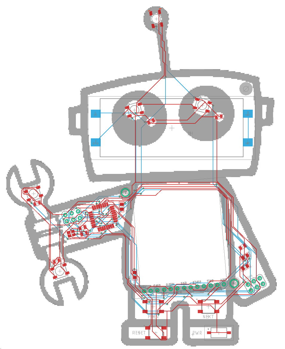
In this part of this series on PCB art design, we plan out the components within the created board design.
Reduce the Alt Grid
For both the schematic design and for the board design, Eagle uses a grid for placing components. As you move parts around the board, they will snap onto the grid. Moving parts normally use a coarse grid size and if you hold Alt while moving parts, your components will snap to a finer grid. The default grid size is 50 mil for the coarse grid and 5 mil for the fine grid.
However, when designing PCB art, you will probably find yourself wanting more granular control over the positions of components. For example, the LED at the top of the antenna on the Maker Pro robot PCB badge needs to go in a very specific location. If that location does not happen to fall exactly on the grid, you will not be able to position the component exactly where it needs to go.
Therefore, when creating artistic PCB designs, it is useful to set up Eagle to use a very fine Alt grid. This will, in effect, give you infinite flexibility for positioning components exactly where they need to go to create an aesthetic design.
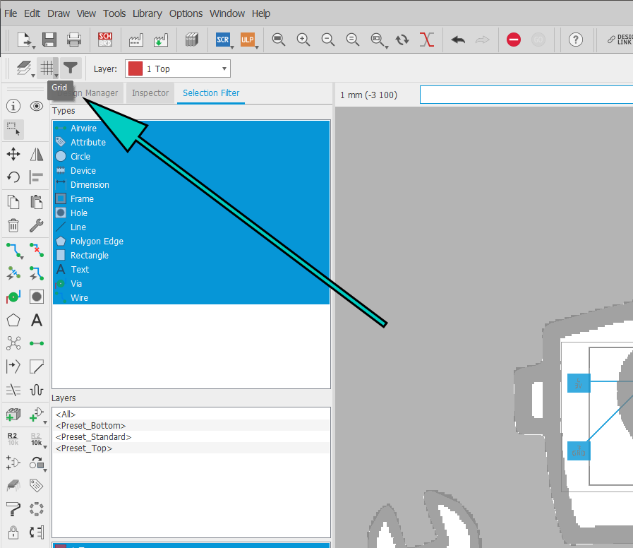
To change the grid setting, click on the Grid icon in the upper-left corner of the window.
Click Grid to change the grid setting
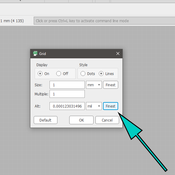
Then, to the right of the Alt: field, click the Finest button. This will set the Alt grid to the smallest distance increment Eagle supports.
Click on Finest to get the smallest distance increments
Finally, press OK to save the settings. Now you will be able to position components in highly specific locations so that they exactly match up with your design. For the Maker Pro robot badge, this is very useful, again, for the LED at the top of the antenna, the LEDs on the robot’s eyes, and the microcontroller and its companion passive components on the robot’s right arm.
Use the ROTATE rX Command
Just like we wanted the flexibility to position components in precise locations on the board, it is also useful to have the ability to rotate components by highly discrete degrees. This can be done for an aesthetic effect, like with the slightly rotated cutout for the eInk display in the middle of the Maker Pro robot badge, or because components need to be rotated in specific ways in order to fit into the design, like with the ATmega328 chip on the robot’s arm.
Here the parts have been rotated to match the axis of the robot’s arm.
Typically, Eagle just rotates components by 90 degrees. It is somewhat common to also use 45-degree rotations to place components on diagonals. However, using the ROTATE command, we can choose any rotation about needed for the design.
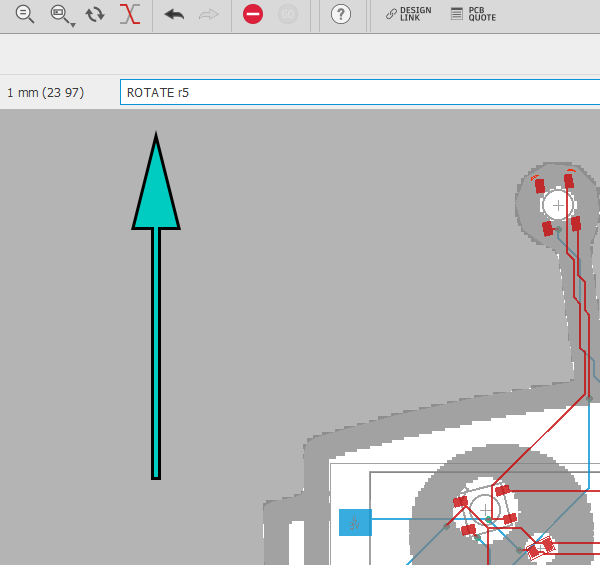
At the top of the Eagle window, there is a text entry field with the placeholder text “Click or press Ctrl+L key to activate command line mode.” The command line allows commands to be input for particular actions, tools, or parameters.
In this case, we will use a command to enable components to be rotated by whatever angle we choose, ROTATE rX, where X denotes the angle to rotate. A positive angle rotates parts clockwise, a negative value rotates parts counterclockwise.
After entering the command, you can simply click on components to rotate them
We Have a Completed Design! Now What?
By using a small grid and making use of the rotation tool in Eagle, we can achieve close to infinite flexibility in the placement of components in the Maker Pro robot PCB design. These techniques allow parts to be positioned in specific places, like the pupils in the robot’s eyes or placed at specific angles, like the angle of the wrench.
At this point, the PCB design is finished. In the next step, we will work on creating the Gerber file and ordering the PCB from a manufacturer.