In this part of this series on custom PCB art design, we send out the Gerber files to finally get the PCB manufactured!
So far, we’ve done a lot of work designing the Maker Pro robot PCB badge. Check out our progress in previous articles to see what went into getting our PCB to this point.
- We created an outline for the PCB by tracing the Maker Pro logo in Adobe Illustrator.
- We created a bitmap image of the graphic elements of the logo that we imported into Autodesk Eagle to create graphics on the PCB.
- We used a similar technique to create bare copper areas on the PCB.
- We created a schematic for the circuit design.
- Finally, we creatively arranged the components on the PCB.
With all of that done, we can finally get the PCB badge manufactured!
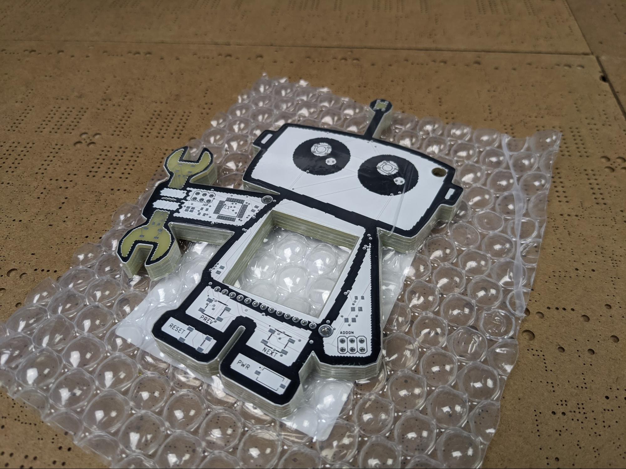
For this project, I used a PCB fabhouse called SeeedStudio Fusion PCB. Seeed offers a lot of flexibility for specifying how your PCB will be made. For the purposes of this tutorial, the wide range of solder mask colors SeeedStudio offers is of particular importance. It is also helpful that the Fusion PCB service fully supports internal cutouts in designs, like the cutout for the eInk display in the middle of the Maker Pro robot badge.
To get a custom PCB created by SeeedStudio Fusion PCB, we have to prep the correct files for manufacturing.
Here’s a preview of the PCBs from SeeedStudio Fusion PCB.
How to Create the Gerber Files
The first step in getting the Maker Pro robot PCB manufactured is creating Gerber format design files from Eagle.
There are, of course, many different options for PCB design software available to makers and engineers. Each has its own internal PCB format; in the case of Autodesk Eagle, we use .SCH files for schematics and .BRD files for boards.
The Gerber format, on the other hand, is a standardized, open format that can be exported from any PCB design software. Gerbers are the standard file format used in the PCB manufacturing industry.
The Gerber format involves a set of files, each containing information about different layers in the PCB design.
In Eagle, open the BRD file for the Maker Pro robot badge. Then, from the toolbar click the CAM Processor button.
Click the CAM processor button.
Then, in the CAM Processor dialog box, click the Load Job File button. A job file is essentially a pre-made script for exporting Gerber files. Fortunately for us, Eagle includes a job file for SeeedStudio Fusion PCB right out of the box.
Load your job profile in CAM processor.
Next, select the Seeed Fusion job file, which is located in System Examples > Third Party > Seeed Fusion > SeeedFusion_2_layer.cam.
Navigate to Seeed Fusion to get the correct job file.
Finally, ensure that the Export as ZIP checkbox at the top of the dialog box is checked. Then, click the Process Job button and choose a location to save your Gerber files.
Check that your file exports as a ZIP and then click Process Job.
Ordering the PCB
With a set of Gerber files in hand, we can order the blank Maker Pro robot PCBs.
We start by heading over to the SeeedStudio Fusion PCB website. At the top of the page, there is a button that will allow you to upload the .zip file containing your Gerber files.
There are a bunch of options for how the PCB will be made. Most of these options will default to the correct values:
- Base Material: FR-4 TG130
- No. of Layers: 2 layers
- PCB Dimensions: 126.1 * 92.1
- PCB Quantity: 5
- No. of Different Designs: 1
- PCB Thickness: 1.6
- PCB Color: White
- Surface Finish: HASL Lead-free
- Minimum Solder Mask Dam: 0.4mm
- Minimum Drill Hole Size: 0.3mm
- Trace Width/Spacing: 6/6 mil
- Blind or Buried Vias: No
- Plated Half-holes.Castellated Holes: No
- Impedance Control: No
The settings on the order form for the PCB.
For a few of these settings, we have a couple options. First of all, the color of the PCB. The color you choose for the soldermask affects two things:
- Obviously, the first thing is the color of the soldermask. For the Maker Pro robot PCB, I chose a white PCB. We will actually be coloring the PCB to match the teal color of the Maker Pro logo so white is the best option available.
- The second aspect of the design affected by the choice of color is the silkscreen color. For all the colors except for white, the silkscreen is printed in white. For white, however, the silkscreen is black. This is advantageous for the Maker Pro robot PCB because all the graphic elements in the logo are black.
Another option worth discussing is the surface finish. For this design, we do not need any overly fancy options like Hard Gold or even ENIG, as the Maker Pro robot badge is not a high-wear part and we are not using any fine-pitch components.
HASL and HASL Lead Free are the most common PCB surface finishes as they perform well and are low-cost. Either option works for the Maker Pro robot PCB but I decided on a HASL lead-free finish. Even though it is slightly more expensive than regular HASL, I prefer not having lead in the PCB.
Review and After the PCBs are Delivered
In this part of the series, we created Gerber files from the PCB design we’ve been working on throughout the first five parts of this article series. Gerbers are the industry-standard file format used for PCB manufacturing. Then, using these Gerber files, we ordered the Maker Pro robot PCB from Seeed Studio Fusion PCB.
It takes a week or two for the PCBs to arrive from Seeed. Once they’re delivered, we will assemble the PCBs with the other components.