PCB art requires technical and artistic skills. Learn how to get your desired PCB shape ready in Adobe Illustrator.
Have you ever started researching a new idea or a new topic that sends you down a rabbit hole into a world you never realized existed? In this article, we will be exploring one such topic: PCB art.
PCB art is a fascinating hobby that combines a wide swath of different technologies and skills: artistry, electrical engineering, component sourcing, programming, soldering, and using design software in ways it was not necessarily intended to be used. The goal is to find innovative ways to design decorative PCBs that incorporate (often interactive) functionality.
This article, the first in our series, covers the history of the PCB art trend and provides step-by-step instructions on how to get your custom image prepped to become a working PCB.
A Brief History of PCB Badges
PCB artwork, and especially PCB conference badges like the ones pictured above, are most closely associated with the annual Def Con and Queercon hacker events.
The #badgelife movement got its start around 2006 when conference attendees interested in hardware hacking had an idea that the attendance badges worn by attendees, press, organizers, and other people at the conferences could themselves be made from PCBs.
The earliest PCB badges were very simple. They featured an artistic board shaped like a skull and crossbones, with LEDs for eyes that blinked in different patterns.
Since then, the badges have become more sophisticated each year.
More recent badges often incorporate dozens of LEDs, highly intricate artistic designs, buttons, wireless connectivity, and small LCD displays. Plus, the most popular badges often contain hidden puzzles and secrets within their programming. By joining together multiple badges, clues are revealed and additional features can be unlocked.
The race to be the first in attendance to figure out these hidden puzzles is a huge part of the attraction to the PCB badges and the feat is often rewarded with exclusive prizes.
Intrigued? Well, even if you can't attend Def Con, you can still make custom PCB art! Let's dive into how you even get started on such an endeavor.
How to Get Started With PCB Badge Design
Creating PCB art is a great outlet for both technical and artistic skills, plus it is a great way to learn new skills. In this article, we will be creating a PCB badge based on the Maker Pro robot logo.
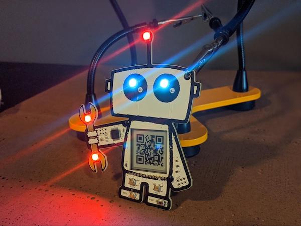
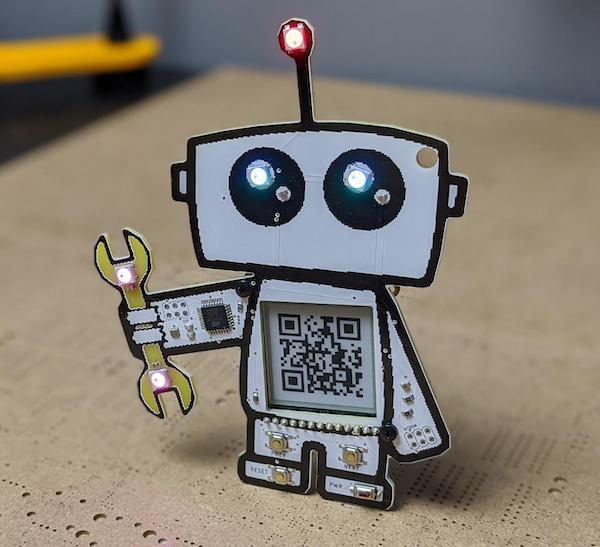
The Maker Pro robot PCB badge complete with LEDs and an eInk display.
A close up of the eInk display on the completed PCB badge.
The completed badge features RGB LEDs, an eInk display that shows a QR code for sharing some of your own or your favorite Maker Pro articles, and some buttons to control the LEDs and the display.
In the process of designing and assembling the badge, we will learn a number of skills and techniques related to various aspects of the design:
- Creating an image on which to base the design
- Creating a complex PCB shape
- Using layers in Eagle to create different colors on the PCB
- Adding graphics to the PCB
- Placing components
- Assembling and programming the board
Creating the PCB Shape
When designing PCBs in Autodesk Eagle, it is easy to make simple board shapes using the built-in drawing tools: rectangles, circles, polygons, and other geometric shapes are all easy to create using the line tool and a bit of geometry. Simple variations on these shapes are also fairly easy to design, like designs with cutouts or rounded corners.
However, PCB art often requires a substantially more complex board outline. The Maker Pro robot PCB we are designing in this tutorial has a fairly complex board outline, not to mention complex internal design elements.
The Maker Pro robot is a complicated shape for PCB design.
While it is certainly possible to draw a shape like this by plotting all of the vertices' Cartesian coordinates, the level of effort required to design the PCB this way is daunting to say the least.
Instead, we will use Adobe Illustrator to create a vector drawing from a reference image, then save the vector drawing in a format that can be imported into Autodesk Eagle.
Tracing the Reference Image in Illustrator
The easiest way to start your design is with some kind of graphic, drawing, or image used as reference material. In this tutorial, we are using an image of the Maker Pro robot logo. You could also use a different image or icon, a drawing or sketch, or even a photograph.
That said, you will have the easiest time with simpler images that have very clean lines and, as much as possible, only solid colors rather than gradients. Simple designs are much easier for Adobe Illustrator to convert into vector graphics.
Our initial image: the Maker Pro robot.
The first step in creating a PCB shape based on the reference image is turning the reference image into a vector drawing. This is done in a process called tracing. Fortunately, Adobe Illustrator has a very capable automated tracing tool that works for most simpler graphics.
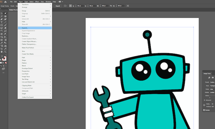
With your reference image open in Adobe Illustrator, select Window > Image Trace to open the trace tool.
Open the Image Trace tool in Illustrator.
Our ultimate purpose in this part of the tutorial is to create a vector drawing that can be imported into Autodesk Eagle and used for the Dimension layer of our PCB art. Therefore, when tracing the image, we want to get the simplest design possible that will still convey the design.
In the tracing tool, there is a Colors slider. Adjust this slider for the minimum value that does not result in lost details of your design. As you adjust the slider, you will see a real-time preview of the tracing result. When you are satisfied with the quality of the trace, press the Trace button to convert your image into the vector graphic.
Use the Colors slider in the tracing tool to simplify the design.
In order to work with the vector drawing, we will need to use the Expand tool. The Expand tool basically makes it so that groups of lines that are not connected to each other are treated as separate shapes. Go to Object > Expand.
Find Object —> Expand in Illustrator.
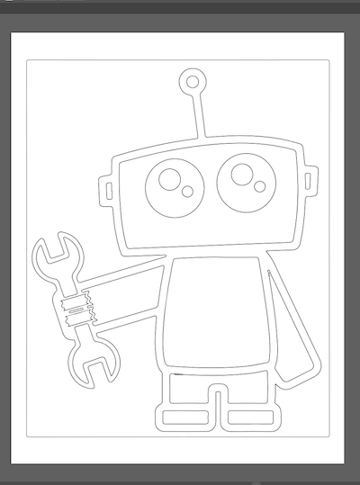
Then, in the dialog box that appears, you will find two checkboxes. Check the Object box and deselect the Fill box.
Select Object and deselect Fill to help further simplify the design.
We will be making a couple changes to the graphic in the appearance toolbar. This is the set of tools for adjusting colors and stroke length. First, select everything in the graphic by dragging a selection window over the entire artboard, then:
Get rid of the fill colors by holding SHIFT and clicking the left color box. Select the white box with the red cross through it to eliminate the fill colors.
Using the Appearance Toolbar
We will be making a couple changes to the graphic in the appearance toolbar. This is the set of tools for adjusting colors and stroke length.
First, select everything in the graphic by dragging a selection window over the entire artboard.
Then get rid of the fill colors by holding SHIFT and clicking the left color box. Select the white box with the red cross through it to eliminate the fill colors.
Get rid of the fill colors.
Next, increase the stroke width to 0.5pt by clicking the up arrow in the Stroke box. Without doing this, the stroke width would be zero, meaning we would not be able to see the lines without selecting them.
Increase the stroke width.
How to Scale the Drawing
So now we have a vector drawing based on our reference Maker Pro robot image! Next, we need to ensure that the drawing is scaled correctly so that the PCB will be the correct size.
In order to accomplish this, we will need some kind of datum points on the design. This can be any element or component of a known size that can be used to adjust the size of the drawing.
In the case of the Maker Pro robot PCB, as mentioned above, there will be an eInk display on the robot’s stomach for displaying a QR code. This display is 28mm x 28mm. Using the Rectangle Tool, click on an empty area of the drawing. This will display a dialog box allowing you to input the exact size of the eInk display.
Create a space for the eInk display using the Rectangle Tool.
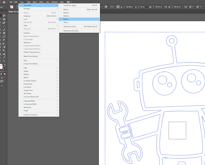
To scale the rest of the drawing, first select everything in the drawing except your datum point shape. Then, select Object > Transform > Scale.
Select Object —> Transform —> Scale.
Then, in the Scale dialog box, adjust the Uniform scale factor until your drawing is the desired size. This might involve some fiddling. For the Maker Pro robot design, I scaled the drawing to 55%.
Scale the image to the correct size (in this case, 55%).
Now that the graphic is the correct size, delete the datum point shape. Then save the image. As we progress further in this tutorial, we will be isolating certain elements of the design but it will be important to maintain a file that contains the entire vector drawing.
Therefore, save any future versions of the image as separate files. If you don’t do this, you will find yourself repeating the image trace over and over.
How to Isolate the Outline
The next step is to isolate the outline of the drawing. This will be used as the Dimension layer in Autodesk Eagle, the outline of the PCNB.
Using the Group Selection Tool, select just the outer perimeter of the drawing.
First, select only the outer perimeter of the drawing.
Then, to select everything except the outline, go to Select > Inverse.
To select everything but the outline, use Inverse.
Finally, simply press delete to remove everything other than the outline of the drawing.
We're left with just the outline of the drawing.
Quick Review and Our Next Steps
PCB art is a hobby that enables makers to create beautiful printed circuit boards that are an expression of both artistic and technical skills.
Often seen at technology-focused exhibitions, PCB badges are a particularly popular example of PCB art. PCB badges feature both elaborate designs and elaborate functionality and are designed to show off the creator’s artistic and technical skills.
What we're working toward in this series.
The first step in creating an artistic PCB from a reference image is converting the outline of the image to a vector graphic.
To do this, we used Adobe Illustrator and its built-in Live Trace tool to automatically create a vector drawing based on a reference image, in this case, the Maker Pro robot logo. In the next part of this series, we will import this vector drawing of the design outline into Autodesk Eagle.