Maker Pro
Maker Pro

Nand Gate oscillator help

KrisBlueNZ

Sadly passed away in 2015
Nov 28, 2011
8,393
Joined
Nov 28, 2011
Messages
8,393
You may have forgotten the diode between pin 11 and the components that follow. If you add it, the circuit will work the way you want - kind of.
 

KrisBlueNZ

Sadly passed away in 2015
Nov 28, 2011
8,393
Joined
Nov 28, 2011
Messages
8,393
This circuit uses two gates as a set-reset latch and will do what you want.

270203.001.GIF
 

Arouse1973

Adam
Dec 18, 2013
5,178
Joined
Dec 18, 2013
Messages
5,178
You may have forgotten the diode between pin 11 and the components that follow. If you add it, the circuit will work the way you want - kind of.

I thought that but his PCB defiantly has the diode.
Adam
 

IC71

Sep 8, 2014
20
Joined
Sep 8, 2014
Messages
20
That circuit isn't going to do what you want. If the contacts drawn next to C1 are a touch switch, they won't do anything because that node in the circuit is driven by pin 11 of the IC. The behaviour you'll get is that when you touch the left hand contacts, the oscillator will run, and when you release them, it will stop. C1 will have no effect.

You can get the behaviour you want. I'll post a diagram shortly.

The "Electronic Circuits for the Evil Genius" book said that the touch switch replacing R2 would make RC1 time off manually. I had the same set up on my bread board and it worked.
 

KrisBlueNZ

Sadly passed away in 2015
Nov 28, 2011
8,393
Joined
Nov 28, 2011
Messages
8,393
Right. If you have a diode between pin 11 and the rest of the circuit, then it will sort of work like an ON/OFF switch, with an undefined timeout. It will be slow to respond to the OFF contacts because the capacitor has to discharge through your finger resistance, and the timeout will be undefined. So you could say that it will work.

Your schematic in post #38 doesn't have that diode. It is there on the circuit board though:

epoint 270203 IMG_3016 annotated.jpg

If that diode is damaged, that would explain the problem you have. It could also be due to ESD damage to U1. So I agree with your electronics teacher.

You can try replacing the diode first because that's easiest. If you replace the 4011, put it in a socket. This should have been done originally. CMOS ICs are easy to damage, especially when you're soldering and unsoldering components that are connected to them.
 

IC71

Sep 8, 2014
20
Joined
Sep 8, 2014
Messages
20
Right. If you have a diode between pin 11 and the rest of the circuit, then it will sort of work like an ON/OFF switch, with an undefined timeout. It will be slow to respond to the OFF contacts because the capacitor has to discharge through your finger resistance, and the timeout will be undefined. So you could say that it will work.

Your schematic in post #38 doesn't have that diode. It is there on the circuit board though:

View attachment 16044

If that diode is damaged, that would explain the problem you have. It could also be due to ESD damage to U1. So I agree with your electronics teacher.

You can try replacing the diode first because that's easiest. If you replace the 4011, put it in a socket. This should have been done originally. CMOS ICs are easy to damage, especially when you're soldering and unsoldering components that are connected to them.
I checked the diode and the reading I got was .583! does that mean it is damaged?
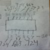
I also checked the 4011 and these are the readings I gotIMG_1209.JPG

Do these readings mean they are busted?

Also, what does ESD and U1 mean?
 

KrisBlueNZ

Sadly passed away in 2015
Nov 28, 2011
8,393
Joined
Nov 28, 2011
Messages
8,393
The diode is probably OK. If you measure it out-of-circuit (removed from the circuit board) using the diode test range on your multimeter, with the black probe to the cathode (stripe end), you should get a reading of around 0.5~0.7V. 0.583V is fine. This voltage is called the "forward voltage" of the diode, and it's the voltage drop across the diode when it is "forward-biased", i.e. conducting.

You can also measure the diode on the resistance range of your multimeter, with the probes reversed - red probe to cathode. It should read open circuit (usually this is shown as something like ".0 L" or similar on the display).

It's hard to tell whether the 4011 is damaged just by looking at the pin voltages. I think it's very likely that it is, though. When you replace it, fit an IC socket, and buy a few spare 4011s, so you can replace it again if necessary.

U1 is the circuit reference for the 4011. Every component has a circuit reference - R1, R2, C1, D1, etc.

ESD is electrostatic discharge. CMOS inputs are easily damaged by very small currents that are generated by voltages that build up on your body, often due to friction (your feet on the floor or on carpet) or certain types of clothes (wool and synthetics). It's possible to build up a charge of hundreds or thousands of volts. Sometimes you will feel it discharge - there's a spark and a pinprick feeling - but not always. These discharges are FATAL to CMOS inputs.

When you're working with CMOS, it's recommended that you wear a wristband that's connected to earth through a high resistance. This keeps your body at ground potential. If the circuit is also kept at ground potential, no electrostatic charge can build up between you and your circuit. Alternatively, you can cover the IC with aluminium foil, or conductive foam, while you're working on the circuit, to ensure that no voltage can form between any of its pins.

Look up ESD using Google or Wikipedia for more information.
 
Top