HellasTechn
- Apr 14, 2013
- 1,579
- Joined
- Apr 14, 2013
- Messages
- 1,579
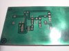
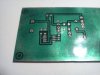
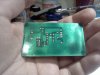
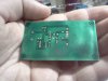
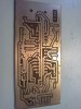
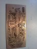
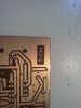
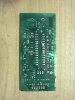
Dear friends,
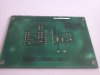
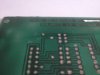
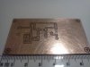
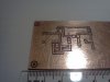
From now on i would like to dedicate this topic to demonstrate The PCB's i have made.
Enjoy !
From now on i would like to dedicate this topic to demonstrate The PCB's i have made.
Enjoy !
Last edited by a moderator:


")