Sir dafa . . . . . . . .
I am working with your
VERY first info
NOW, but I see that you added in
ONE good pic . . .the first one . . . about the 12 V presence, lets go with expecting that voltage level, as supply voltage over in your "
RED ARROW " area.
So I now continue on, with your first post.
Well the NordicTrack 1750 units book tells me that the display is using a 10 in tablet for its display . . . . but not what connections are needed from that display to the rest of the unit. Possibly just that USB connector ? and are you using the proper port ?
OTG ?
S o o o o o o o in just going with your board corner that you were initially showing us, let me just initially work with that.
You have concentrated on the top left corner of that board and that seems to be dedicated to creating two + and - polarities of power supplies at a current capability of ~ 300 ma if so needed. You will be finding out those voltage values when you test . . .
IF they are there..
Now, with your initial fixation on that specific diode, and its junction voltage reading . . . . . reveals :
I get 1.762V one way and 0.151V the other way.
One might expect a lowest 0.500 V through 0.700 V highest reading on common silicon diodes being used in that application.
BUT, your 0.151 reading, falls right in line with a Schottky family diode, and your 1.762V reading is
PROBABLY fully attributable to circuitry that is also shunting
across that diode.
To be sure, one needs to lift one leg / terminal completely out of circuit to test that way.
BUT since that is a surface mount, it would require a heating of both tabs and getting the solder molten . . .and
THEN the grip in the center with a pair of tweezers to enact an ~ 45-90 degree twist on the body to break the adhesive under the diode to the PCB loose . . . then you are broken Free . . . .
FREE AT LAST !
BUT . . .
BUT . . . .
BUT ! . . . . I would not ask you to do that , for your then finding out my 99 86 / 100 ths
% suspicion of that unit being absolutely and totally O.K. ( Remember those 0.151 magical numbers ? )
Instead, lets consult the application note / schematic that TI provided for their little gem of a dual voltage converter.
INFORMATION CENTRAL . . .is now . . . PRESENTING to you . . . . . .Ta Da . . . . .

Study this schematic and initially note input power comes in to top left corners V1
GREEN A position and then routes to Q1 power switching FET and to pin 5 or 6
Green B of Tipsy 65130 Eye See. This feeds an internal FET for your negative supply portion.
Also note the power branch thru pi filter of C2 - R7 - C3 and on to pin 4
Green C of the IC.
VOLTAGE CONVERSION . . . . . OPERATIONAL RUNDOWN . . . .
Using the
PINK markup of the Positive supply, and we will assume that +12 that you have already found on the board will be coming in to
GREEN A and then to S of Q1 and wanting to pass thru to D . . . . but no can do until gate activation.
But, a stream of pulses are coming to that gate from pin 7 BSW.
Specifically at 1,250,000 pulses per second . . . . .on upwardly to 1,500,000 PPS, in accordance to PS operating conditions.
You might say we have ourselves a pulse train there, with no
WAITING at the station, but you may have one
HARD time picking out
YOUR train.
(
PLUS . . . . Man that's being one HELL of a LOT of pulse " trains " per second ! )
HEY ! lets keep going on with this train analogy.
As for the POWER supplied by these trains, relate that to the number of box cars pulled with their "energy", a train might have as many as its 87 boxcar pulling limit or as short as 12 cars. ( 87% pulse width or 12% pulse width. )
So we now have the individual pulses coming in to the Q1 gate and it has its gate turned on for the required duration of that pulse ( a train and its box cars)
That Q1 conduction is letting the
REAL energy coming in from that 12V supply, be fed into the L1 inductor which starts building up a magnetic field proportionally to the incoming pulses width (duration). At the instant that the pulse ends Q1 stops power flow due to no gate drive.
BUT that strong magnetic field having been created within the L1 inductor, then collapses, and the falling magnetic field creates a strong back EMF, ringing waveform as can be seen illustrated in the RED asterisk inset. D1 diode then captures that energy to pass on down to C4 storage cap / filter down near the
GREEN G at the right top end of the schema.
As C4 it is building up its stored voltage, a simultaneous sampling it taking place at
GREEN E , where R1 / R2 voltage dividers center junction send out a voltage to
GREEN K at FBN.
FBN then sends any required correction to the oscillator and Schmitt trigger portions of the pulse generator, that feed into BSW gate drive to alter either / and / or its frequency or pulse width.
( Slow down the number of trains and /or their numbers of box cars. )
Same procedure down at the
BLUE portion of the schematic for the negative supply, excluding the "Q1" equivalent, which is being
internal of the IC. Its corrective voltage sampling is from
GREEN J and feeds down to the R4-R3 voltage divider junction which feeds to
GREEN K , so that it can make corrections to its FET driver.
YOUR TASK AT HAND NOW . . . . .
You now just need to find 4 test points, and as close as those IC terminals are . . . .even with needle probes, and YES I do use soldered on needles for a set of my probes.
Best you have a DEAD non powered board and use the supplemental IC basing I added at the bottom with its dimple in the chip corner pin 1 marker, and count around.
Pin 2 or 3 will give you ground, and an ohmming around the board should find another connector with somewhat GREATER SURFACE area to place your - meter probe on.
Pin 5-6 , the same way, in finding that SAME connection but on larger real estate.
Pin 23 will give you this units + power out or any of the also connected terminals of C4's equivalent on this board or preferably D1 equivalency.
Pin 15 will give the negative supply from the unit.
I would mark and identify those alternate test points on the board with a mini Sharpie.
Then its power up and put meter ground to your preferred ground alternate and then probe power in to see if this is using +12 v input . . . and then . . .and then . . .
and then . . . do we have the supply's + and - outputs ?
OBSERVATIONS . . . .
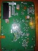
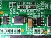
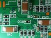
Looking around and about your very first photo.
We have your red arrow and the nearby L13 and another L17, items, I perceive both as strip line thru ferrite bead RF / EMI chokes.
That is then leaving the bulky round L18 as being our L1 equivalent ringing choke for the + supply.
Just below it is a "U37" which I really think is being a power FET, with enough support circuitry inside, as to deem its IC classification . . .U identifier . . .vice Q for a transistor.
Top and left of L18 is D14 which, by its proximity, I would deem as being that inductors associated diode . . .your D4 is being TOO far away, as per defying good design practice .
Find your IC pin 1 dimple and it points down to L16, as I suspicion to be our other ringing inductor for the negative supply.
D9, just above it, seems to relate as its associated diode.
I am wanting to think that the CA 35, just below L13 is being a monolithic high density X7R ceramic capacitor for that C4 equivalency main storage cap for the + supply.
If you find those + and - voltages being present, then check both sides of
YOUR RED D4, just to see if it might be associated with the 12 VDC supply that you are finding present.
I now stop . . . . to let you update me.
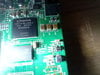
Here's your U10 . . . . . Da Da sheet
https://www.digikey.com/htmldatasheets/production/1785837/0/0/1/nb634-datasheet.html
What supply voltage is being found at its pin 1 ?
73's de Edd . . . . .
Now I may not be as funny or athletic or good looking or smart or talented or experienced or rich or wise or . . . . . . . . ??? . . . . . drat, I forgot where I was going with this.
.


")